ALLPCB


Power demands and duty cycling
Power-delivery environments for wearables and other devices used in the Internet of Things (IoT) are complex. Because energy must be conserved whenever possible, power consumption varies widely. Typically, IoT devices spend most of their time in sleep states to achieve minimum power draw and are only awakened when measurements must be taken or data transmitted. Wake-up modes themselves can differ significantly.
For example, only a small subset of subsystems may need to wake to sample an A/D converter that periodically reads sensors. However, when data is sent over a wireless link such as Bluetooth Smart, most devices from the processor to the radio front end must be active and consume relatively high power.
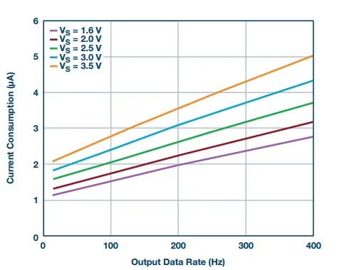
Although Bluetooth Smart reduces overall power consumption, its low-power mode still draws about 15 mA, while the high-data-rate mode requires 30 mW. Supporting these modes means that the PMIC must be able to switch rapidly from an ultra-low standby state to deliver several milliseconds of high current, then turn the system off again just as quickly. This places stringent demands on power delivery.
When a processor moves from one of its lowest-power sleep states to an active mode, the change in current requires fast turn-on and transient response from the power-delivery subsystem.
Processors used in IoT gateways and hubs also show a wide range of power behavior. Although they spend less time in sleep modes, processors designed for these applications often use dynamic clocking and voltage-scaling strategies to match power to workload. As a result, current can vary significantly and transitions between modes occur rapidly.
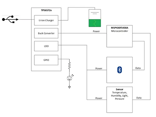
Figure 1: Block diagram of a typical communications-centered IoT or wearable device based on TI power and MCU components.
Control strategies and transient response
The demand for fast transient response can stretch the capabilities of conventional pulse-width modulation (PWM) closed-loop control strategies used in DC/DC converters. Typically, a PWM circuit generates a small error signal by subtracting a scaled version of the converter output from a reference voltage. That error signal is compared with a conventional ramp driven by an oscillator that usually runs at a fixed frequency. A comparator outputs a digital signal that operates the power switch.
When the output voltage changes, the error signal changes and the comparator threshold shifts. Consequently, the output pulse width changes. That duty-cycle change moves the output voltage so that the error signal is reduced toward zero, completing the control loop.
Basic PWM strategies have many advantages, but to ensure stability the closed-loop control bandwidth is usually kept relatively low—often an order of magnitude below the PWM switching frequency. Therefore, transient response can be limited.
Hysteretic control and fast transients
Hysteretic control offers a faster alternative. In its simplest form, the controller is a comparator with a small hysteresis between its two inputs. One input is the converter output voltage, the other is the reference. When output voltage drops due to increased load current, the comparator produces a high output, activating the gate driver for the main output transistor and supplying the load. The output voltage rises until it exceeds the hysteresis margin around the reference, at which point the comparator turns the gate driver off.
Because there is no slow loop amplifier to filter the signal, delay between output voltage changes is limited to comparator propagation and gate-driver delays. Hysteretic control therefore provides very fast transient response. Another advantage is that hysteretic control naturally supports wide variations in load current, from sub-milliamp ranges to peak currents exceeding 1 A.
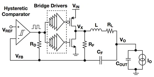
Figure 2: Schematic of a hysteretic power controller.
This flexibility comes at the cost of large variations in switching frequency, which can cause electromagnetic compatibility (EMC) issues and stimulate resonances in passive networks around the power rails. Output-voltage accuracy can also be lower, which may be a concern for voltage-sensitive microcontrollers and sensors.
Hybrid converters for low-load efficiency and predictable frequency
Hybrid converters combine both strategies: a hysteretic comparator controls low-load rails typical in deep sleep and low-power modes, and the converter switches to traditional PWM once load current exceeds a set threshold. This provides both the low-load efficiency and fast response of hysteretic control and the predictable frequency and efficiency of PWM under heavier loads. One example is the LM2650M synchronous buck DC/DC converter from Texas Instruments, which operates across load ranges from milliamp levels up to 3 A. The device also offers a logic-controlled shutdown mode in which the input supply can draw up to 25 μA.
The LM2650 uses fixed-frequency PWM and synchronous rectification to achieve high efficiency at higher loads. In many applications, efficiency exceeds 95% at around 1 A, and remains above 90% for medium to heavy loads from 0.2 A to 2 A. At lower loads, the device enters a hysteretic sleep mode. The LM2650 automatically enters and exits sleep based on a separately programmed current threshold, and an external resistor provides hysteresis for the mode switch.
In hysteretic mode the LM2650 uses a built-in comparator with 30 mV of hysteresis centered at 1.25 V. Because hysteretic mode only operates at low load, switching frequency can range from a few hertz to several kilohertz. An optional soft-start feature limits inrush current at startup and provides a simple method for sequencing multiple supplies.
There is a trade-off between noise and the power savings of hysteretic operation. Filtering is easier for fixed-frequency converters for EMC reasons. Therefore, a logic input allows the user to override automatic sleep and hold the LM2650 in PWM mode regardless of load level.
Low-noise converters and system control
Designed for low-noise IoT devices such as fitness wearables, the TPS65720 from Texas Instruments can be commanded via its built-in I2C interface to operate in the low-power hysteretic mode or to force fixed-frequency PWM mode. However, if the system does not sample noise-sensitive analog inputs or operate a radio interface, low-noise performance in low-power mode may not be critical—local high-frequency interference spikes can dominate. Whenever noise-sensitive operation is required, designers can force the device into a low-noise PWM mode via system software to optimize overall energy efficiency.
Running the PWM mode at 2.25 MHz allows the use of smaller inductors and capacitors than would be required at the core switching frequency. As a result, when typical 0402 packages are used for resistors and capacitors, the total footprint of external components can be reduced to less than 11 mm2. The higher frequency also improves transient response and allows the use of high-Q band-pass filters to suppress parasitic frequencies.
The IC also provides a 200 mA low-dropout regulator (LDO) with an input range of 1.8 to 5.6 V, allowing it to be powered from the buck converter output or directly from the system voltage. For devices that only need minimal power, the IC supports shutdown currents below 1 μA, for example to power a real-time clock counting down to the next sensor sampling period.
Conclusion
As IoT designs evolve, attention to transient performance and efficiency in DC/DC converters' low-power modes will increase. Devices such as the LM2650 and TPS65720 offer practical building blocks for meeting the conflicting demands of low quiescent power, fast transient response, and controlled noise in wearable and IoT applications.