ALLPCB


Overview
Microchip dsPIC33FJ06GS101/X02 and dsPIC33FJ16GSX02/X04 combine DSP functionality with a high-performance 16-bit microcontroller architecture. They can reach up to 40 MIPS at 3.0–3.6 V, provide about 35 programmable digital I/O pins, and include 16 KB of flash. The dsPIC33F family integrates high-speed PWM, an interrupt controller, high-speed comparators, a 10-bit ADC, and a range of peripherals. Typical applications include power line communication for electricity meters, home energy monitoring, and smart grid systems. The power-line modem (PLM) PICtail Plus daughtercard provides schematics, a bill of materials, and PCB component placement for a PLM front end.
Devices and DSP/MCU Capabilities
The dsPIC33FJ06GS101/X02 and dsPIC33FJ16GSX02/X04 devices offer extensive digital signal controller (DSC) features along with a high-performance 16-bit microcontroller architecture.
Key Features
- Operating range:
- Up to 40 MIPS operation (at 3.0–3.6 V)
- Industrial temperature range: -40 C to +85 C
- Extended temperature range: -40 C to +125 C
- High-performance DSC CPU:
- Improved Harvard architecture
- C-compiler optimized instruction set
- 16-bit data path
- 24-bit instruction width; linear program memory addressing up to 4M instructions
- Linear data memory addressing up to 64 KB
- 83 basic instructions: mostly 1 word/1 cycle
- Two 40-bit accumulators with rounding and saturation options
- Flexible addressing modes: indirect, modulo, bit-reverse
- Software stack
- 16x16 fractional/integer multiply
- 32/16 and 16/16 divide operations
- Single-cycle multiply-and-accumulate with accumulator writeback and dual data fetch
- Shift capability up to 40 bits with +/-16-bit shift amount
Digital I/O
- Peripheral pin select functionality
- Up to 35 programmable digital I/O pins
- Wake-on-change interrupts on up to 30 pins
- Output pins driven from 3.0 V to 3.6 V
- 5 V-tolerant outputs with open-drain configuration
- 5 V-tolerant digital inputs (except RB5)
- 16 mA source/sink on all PWM pins
Memory
- Flash program memory up to 16 KB
- Data SRAM up to 2 KB
- Flash program memories with appropriate protection
Timers and Peripherals
- Timers/counters: up to three 16-bit timers, which can be paired to form a 32-bit timer
- Input capture: up to two channels, capture on rising, falling, or both edges; 16-bit capture input with 4-deep FIFO per capture
- Output compare: up to two channels; single or dual 16-bit compare; 16-bit center-aligned PWM mode
- 4-wire SPI:
- Frame support for simple codec I/O interface
- 1-deep FIFO buffer
- Supports 8-bit and 16-bit data
- Supports all serial clock formats and sampling modes
- I2C:
- Full multi-master and slave support
- 7-bit and 10-bit addressing
- Bus collision detection and arbitration
- Integrated signal conditioning
- Slave address masking
- UART:
- Address bit detection
- Error interrupts for UART
- Wake from sleep using start bit
- 4-character TX and RX FIFO buffers
- LIN bus support
- IrDA encoding/decoding in hardware
- High-speed baud rate mode
- Hardware CTS and RTS support
Interrupt Controller
- 5-cycle latency
- Up to 35 interrupt sources
- Up to 3 external interrupts
- Seven programmable priority levels
- Four processor exceptions
High-speed PWM Module
- Up to 4 PWM generators with 4 to 8 outputs
- Each of 8 PWM outputs has its own time base and duty cycle
- Dead time for rising and falling edges
- Duty-cycle resolution: 1.04 ns
- Dead-time resolution: 1.04 ns
- Phase-shift resolution: 1.04 ns
- Frequency resolution: 1.04 ns
- Supported PWM modes:
- Standard edge-aligned
- Truly independent outputs
- Complementary
- Center-aligned
- Push-pull
- Multi-phase
- Variable phase
- Fixed off-time
- Current reset
- Current limiting
- Independent fault/current-limit inputs for each of the 8 PWM outputs
- Output commutation control
- Special event triggers
- PWM capture capability
- Prescaler for input clock
- Dual trigger from PWM to ADC
- PWMxL/PWMxH output swapping
- PWM4H/PWM4L remappable
- Dynamic changes to PWM frequency, duty cycle, and phase
- Disable individual PWM generators
- Leading-edge blanking (LEB) functionality
Analog Comparators and ADC
- High-speed analog comparators:
- Up to four comparators with 20 ns response time
- Each comparator has a 10-bit DAC; DAC outputs available on DACOUT pins
- Programmable output polarity and selectable inputs
- ADC sampling and conversion capability
- PWM module interface for duty-cycle and period control and fault detection
- High-speed 10-bit ADC:
- 10-bit resolution
- Up to 12 input channels divided into 6 conversion pairs
- Two internal reference voltage monitor inputs in pairs
- Successive approximation register (SAR) converters for parallel conversion of analog pairs:
- 4 Msps for devices with two SARs
- 2 Msps for devices with one SAR
- Dedicated result buffers per analog channel
- Independent trigger sources per analog input conversion pair
Power and System Management
- On-chip 2.5 V regulator
- Real-time switching between clock sources with fast wake-up
- CMOS flash technology with idle, sleep, and standby modes:
- Low-power, high-speed flash
- Full-static design
- 3.3 V (±10%) operating voltage
- Industrial and extended temperature options
- Flexible clock options:
- External, crystal, resonator, internal RC
- Phase-locked loop (PLL) with 120 MHz VCO
- Main crystal oscillator range: 3 MHz to 40 MHz
- Internal low-power RC (LPRC) at 32 kHz
- Internal fast RC (FRC) at 7.37 MHz
- Power-on reset (POR) and brown-out reset (BOR)
- Power-up timer (PWRT) and oscillator start-up timer (OST)
- Watchdog timer with RC oscillator
- Fail-safe clock monitor (FSCM)
- Reset from multiple sources
- In-circuit serial programming (ICSP)
- Reference oscillator output
Applications
- AC-to-DC converters
- Automotive HID
- Battery chargers
- DC-DC converters
- Digital lighting
- Induction cooking
- LED ballasts
- Renewable power and pure sine-wave inverters
- Uninterruptible power supplies (UPS)
Packages
- 18-pin SOIC
- 28-pin SPDIP / SOIC / QFN
- 44-pin TQFP / QFN
Figures
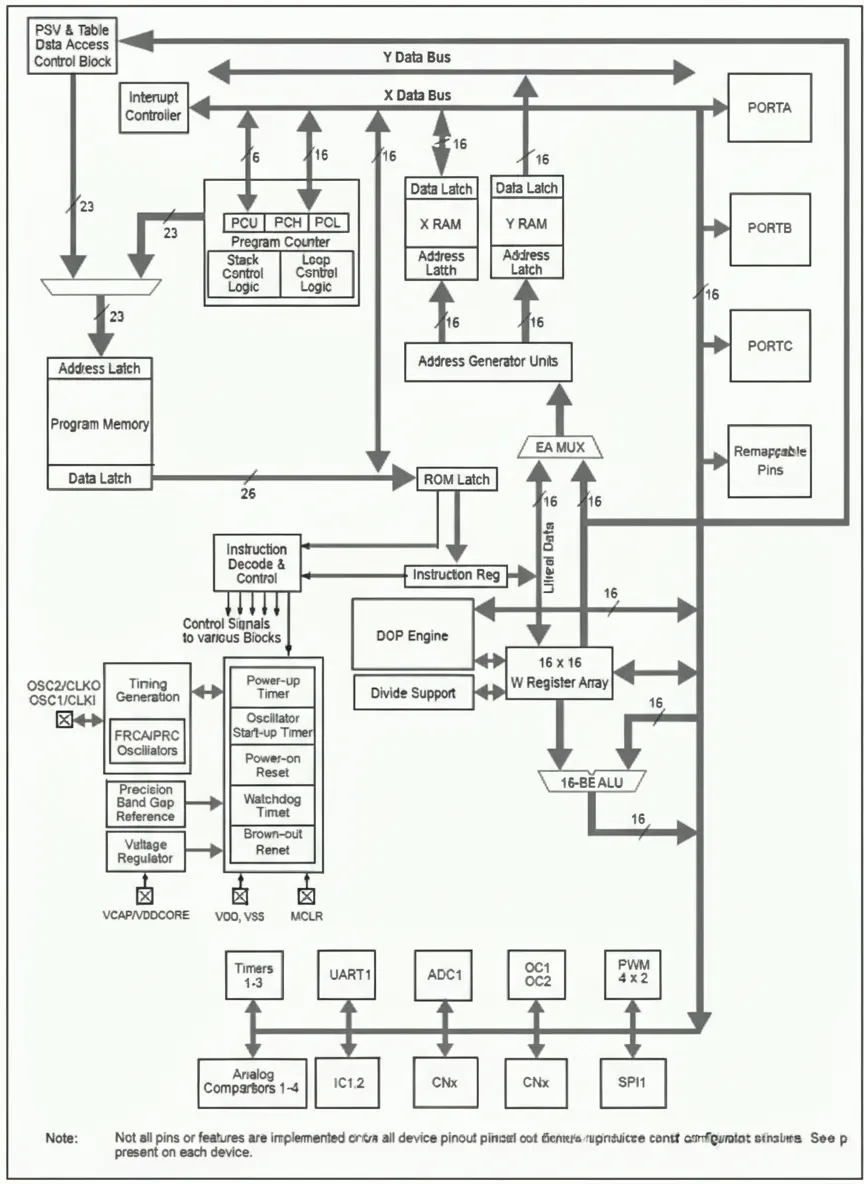
Figure 1. dsPIC33F side view
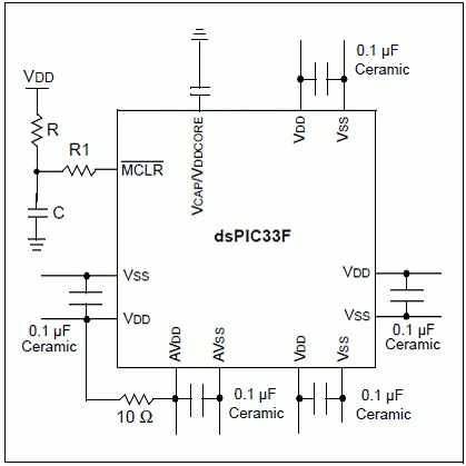
Figure 2. Recommended minimum connections for dsPIC33F
Power-line Modem (PLM) Overview
The power-line modem (PLM), also known as power-line communication (PLC) modem, uses existing power lines as a cost-effective communication medium. This technology supports a wide range of applications including automatic meter reading (AMR), per-device energy monitoring, and lighting, heating, and solar applications. The data rate and robustness of the PLC link determine the suitable application range.
BPSK 6.0 kbps PLM PICtail Plus Daughtercard
The BPSK 6.0 kbps PLM PICtail Plus daughtercard integrates the analog front-end (AFE) required for a software-based modem implemented on a dsPIC33F digital signal controller (DSC) on an Explorer 16 development board. The daughtercard plugs into an expansion socket on the Explorer 16. The HV adapter cable included in the kit connects the daughtercard to the power line and includes the circuits needed for noise filtering and isolation. The daughtercard and HV adapter cable are designed to operate at 72 kHz (CENELEC-A band).
The daughtercard does not implement any particular modulation method in hardware. The dsPIC33F DSC generates four PWM channels in software. When summed and properly filtered by the daughtercard circuitry, these PWM outputs approximate a sine wave. BPSK modulation is implemented in software by controlling the PWM channels. On the receive path, the modulated signal on the power line is filtered and amplified by the daughtercard before being presented to the ADC input of the dsPIC33F DSC. The ADC module converts the received signal to the digital domain, where additional software filtering and demodulation recover the data.
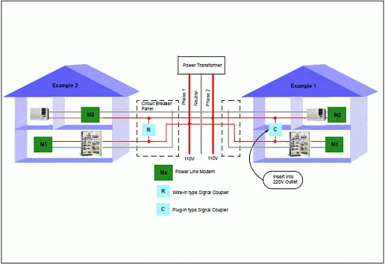
Figure 3. Power-line BPSK application example
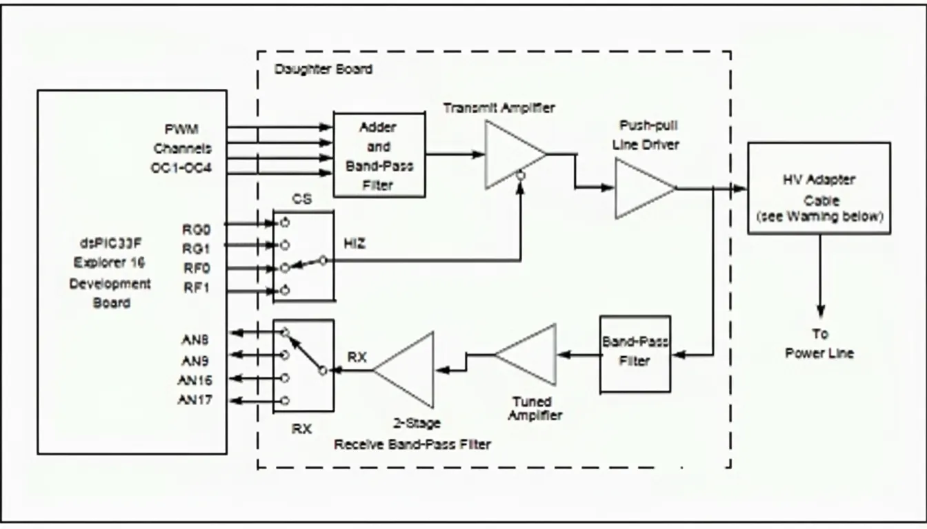
Figure 4. dsPIC33F BPSK 6.0 kbps PLM PICtail Plus daughtercard
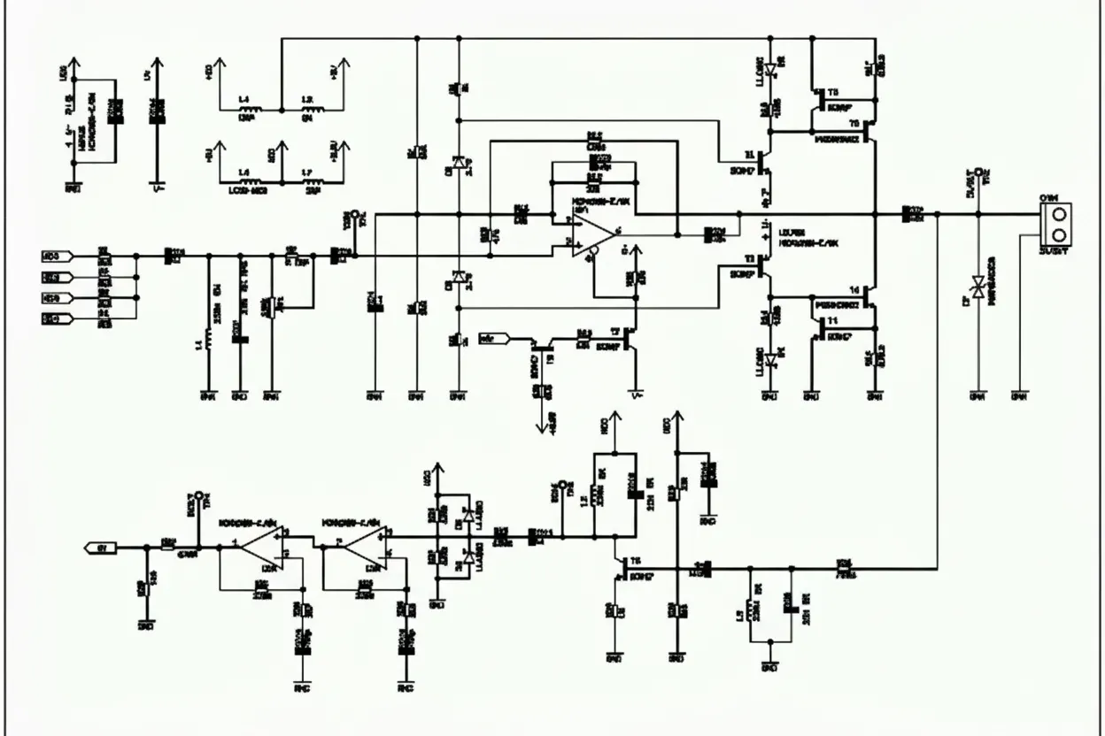
Figure 5. dsPIC33F PLM daughtercard schematic (1)
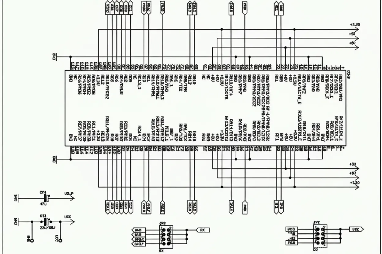
Figure 6. dsPIC33F PLM daughtercard schematic (2)
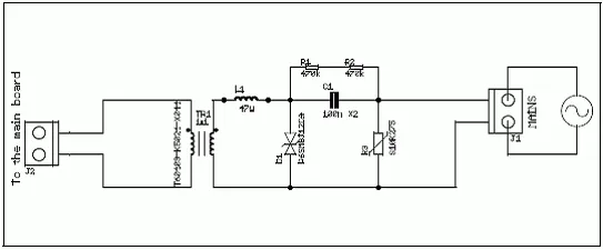
Figure 7. dsPIC33F HV adapter schematic
Bill of Materials and Layout
Below are images showing the daughtercard bill of materials and component placement.
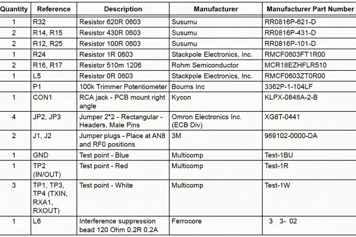
HV adapter bill of materials:
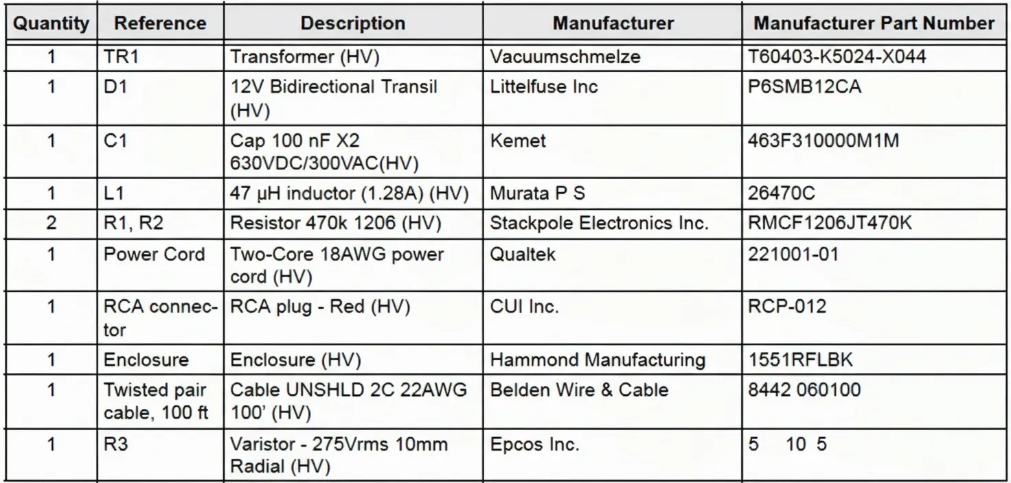
Figure 8. dsPIC33F PLM daughtercard component placement