If you're looking to boost your PCB performance, reduce EMI, and ensure solid signal integrity, mastering copper pour techniques is a game-changer. In this guide, we'll dive deep into how copper pour can optimize power distribution, minimize electromagnetic interference (EMI), and enhance overall PCB design. Whether you're a beginner or a seasoned engineer, you'll find practical tips and detailed insights to improve your next project.
What Is Copper Pour and Why Does It Matter for PCB Design?
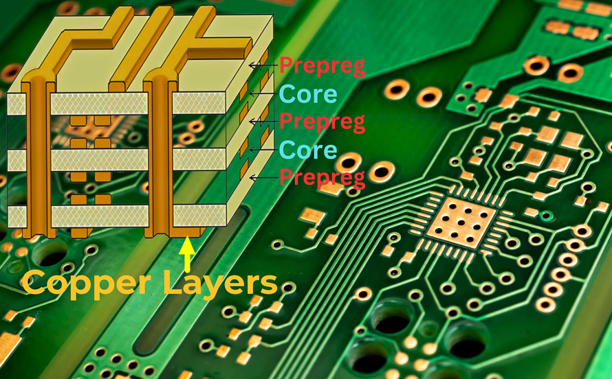
Copper pour refers to the process of filling unused areas of a printed circuit board (PCB) with copper. This technique is often used to create ground planes or power planes, ensuring a more stable and efficient design. But why is it so important? Copper pour plays a critical role in PCB performance improvement, EMI reduction, signal integrity, and power distribution. By filling empty spaces with copper, you reduce noise, improve thermal management, and provide a low-impedance path for current flow.
In modern electronics, where devices operate at higher frequencies (often exceeding 1 GHz), the risk of interference and signal degradation is high. A well-executed copper pour can act as a shield, minimizing crosstalk and ensuring cleaner signals. Let’s explore how to use copper pour effectively and why it’s a must-have in your design toolkit.
The Benefits of Copper Pour for PCB Performance Improvement
Using copper pour techniques offers several advantages that directly impact the performance of your PCB. Here’s a breakdown of the key benefits:
- Enhanced Signal Integrity: Copper pour, especially when used as a ground plane, provides a return path for signals, reducing loop inductance. For high-speed signals (above 100 MHz), this can lower signal distortion and ensure data integrity.
- EMI Reduction: A solid copper plane acts as a Faraday cage, blocking external electromagnetic interference and containing internal noise. This is critical for designs operating in noisy environments or with strict compliance standards like FCC or CE.
- Better Power Distribution: Copper pour creates a low-resistance path for power delivery, reducing voltage drops across the board. For instance, a power plane with a copper thickness of 1 oz/ft2 can handle currents up to 10A with minimal loss.
- Improved Thermal Management: Copper is an excellent conductor of heat. A well-designed pour can dissipate heat from high-power components, keeping temperatures in check and extending component lifespan.
By addressing these factors, copper pour directly contributes to a more reliable and efficient PCB design, making it a cornerstone of modern electronics.
Copper Pour Techniques for Optimal Results
Implementing copper pour isn’t just about flooding a board with copper; it requires careful planning and execution. Below are proven copper pour techniques to maximize PCB performance improvement.
1. Use Ground Planes for EMI Reduction
One of the most common uses of copper pour is creating a ground plane. A continuous ground plane under signal traces reduces the loop area for return currents, cutting down on EMI. For multilayer boards, dedicate an entire layer to ground and connect it to the top and bottom layers using vias. This technique can reduce EMI by up to 20 dB in high-frequency designs (above 500 MHz).
Tip: Avoid splitting ground planes unless absolutely necessary, as splits can create high-impedance paths and increase noise.
2. Optimize Power Planes for Power Distribution
For power distribution, copper pour can be used to create power planes. These planes deliver stable voltage to components with minimal resistance. Use a thick copper layer (e.g., 2 oz/ft2) for high-current applications to handle loads without overheating. Place decoupling capacitors close to power pins and connect them directly to the power and ground planes with short traces or vias to minimize inductance.
Tip: Separate power planes for different voltage levels (e.g., 3.3V and 5V) to prevent crosstalk between power domains.
3. Implement Via Stitching for Signal Integrity
Via stitching involves placing multiple vias around the edges of a copper pour to connect it to other layers, typically ground planes. This technique ensures a low-impedance connection between layers, reducing noise and improving signal integrity. For high-speed designs, space vias at intervals of λ/20 (where λ is the wavelength of the highest frequency signal) to prevent resonance. For a 1 GHz signal, this translates to vias spaced roughly every 15 mm.
Tip: Use via stitching around the perimeter of the board and near high-speed components to create a robust shield against EMI.
4. Balance Copper Distribution for Manufacturability
Uneven copper distribution can cause issues during manufacturing, such as warping or uneven etching. To avoid this, balance copper pour across all layers. If one side of the board has a large copper area, mirror a similar pour on the opposite side. Some design tools allow you to calculate copper density, aiming for a balance within 10-15% between layers.
Tip: Use cross-hatching (a grid pattern) for copper pour in areas where full coverage isn’t needed. This reduces material use while maintaining balance.
Best Practices for Copper Pour in PCB Design
To get the most out of copper pour, follow these best practices tailored for EMI reduction, signal integrity, and overall performance.
- Keep Clearances in Check: Maintain a clearance of at least 0.2 mm between copper pour and signal traces to prevent unintended coupling or shorts. Adjust this based on your board’s manufacturing tolerances.
- Avoid Isolated Copper Islands: Small, unconnected patches of copper can act as antennas, picking up or radiating noise. Ensure all poured areas are connected to a net (like ground or power).
- Prioritize High-Speed Signals: For traces carrying signals above 100 MHz, place a ground pour directly beneath them on the adjacent layer. This minimizes impedance mismatches, keeping characteristic impedance close to the desired value (often 50 ohms for RF designs).
- Use Thermal Reliefs for Soldering: When connecting pads to a large copper pour, add thermal reliefs (spokes of copper) to prevent heat dissipation during soldering. This ensures proper solder joint formation.
Common Mistakes to Avoid with Copper Pour
Even with the best intentions, mistakes in copper pour implementation can hurt your design. Here are pitfalls to watch out for:
- Overloading Copper Areas: Pouring copper without considering current capacity can lead to overheating. Always calculate the required copper thickness based on current draw (e.g., use IPC-2221 standards for trace width and thickness).
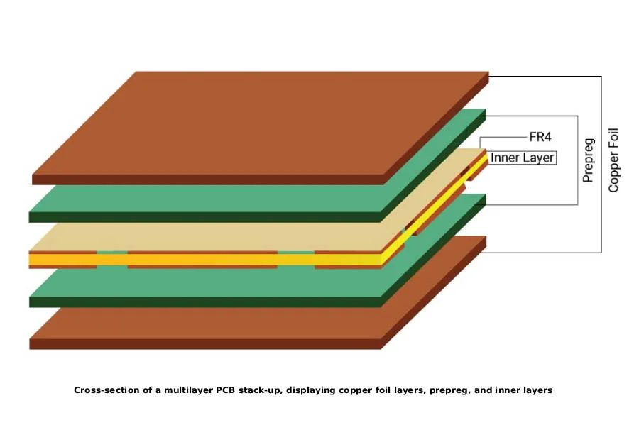
- Ignoring Layer Stackup: Failing to align copper pour with your layer stackup can disrupt signal return paths. For a 4-layer board, a common stackup is signal-ground-power-signal, ensuring ground and power planes are adjacent for low impedance.
- Neglecting EMI Testing: Don’t assume a copper pour will solve all EMI issues. Simulate your design using tools like SPICE or field solvers to predict EMI behavior before fabrication.
Advanced Tips for Copper Pour in High-Speed Designs
For high-speed PCBs, copper pour becomes even more critical. Here are advanced strategies to elevate your design:
- Control Impedance with Copper Planes: Use copper pour to create reference planes for controlled impedance traces. For a 50-ohm trace on a 1.6 mm FR4 board, ensure the ground plane is directly below with a dielectric height of about 0.2 mm for tight coupling.
- Minimize Crosstalk: Place ground pour between adjacent high-speed traces to act as a shield. This can reduce crosstalk by up to 30% in densely packed designs.
- Use Split Planes Carefully: If you must split a plane for analog and digital grounds, connect them at a single point near the power entry to avoid ground loops. Add a small capacitor (e.g., 0.1 μF) across the split to filter high-frequency noise.
How Copper Pour Impacts EMI Reduction and Compliance
Electromagnetic interference is a major concern for PCB designers, especially with strict regulatory standards. Copper pour is a powerful tool for EMI reduction. A solid ground plane can reduce radiated emissions by providing a low-impedance path for return currents, preventing them from radiating as noise. Studies show that a continuous ground plane can lower emissions by 10-15 dB compared to a design without one.
Additionally, copper pour helps with conducted EMI. By connecting the pour to a chassis ground through mounting holes, you can divert noise away from sensitive components. For compliance with standards like CISPR 32, ensure your copper pour covers at least 80% of the board area on ground layers.
Conclusion: Elevate Your PCB Design with Copper Pour Mastery
Mastering copper pour techniques is essential for achieving PCB performance improvement, EMI reduction, signal integrity, and efficient power distribution. From creating ground planes to optimizing via stitching, every step in the copper pour process can make or break your design. By following the strategies and best practices outlined in this guide, you can build reliable, high-performing PCBs that meet the demands of modern electronics.
Start incorporating copper pour into your next project with a clear plan. Focus on balancing copper distribution, prioritizing signal integrity, and testing for EMI. With these techniques, you’ll be well on your way to designing boards that stand out for their performance and reliability.
 ALLPCB


