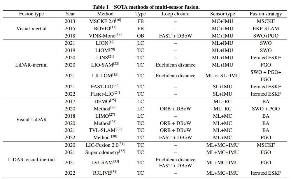
ALLPCB


Resolution (Number of Pixels)
MP stands for megapixel, commonly 0.3M, 1M, 2M, 5M, 13M, 20M, 40M, 100M, etc. Pixel count and resolution are closely related: the combination determines image data volume. For images of the same size, higher resolution contains more pixels. Total pixel count is the sum of all pixels and is a primary technical metric for CMOS image sensors. Effective pixels are those used for photoconversion and image output; the effective pixel count is a subset of the total pixel count and directly determines the sensor's resolving power.
Optical Format
The larger the optical format, the larger the imaging system can be, the more photons it can capture, and the better the light sensitivity and signal-to-noise ratio. Common CMOS optical formats include 1 inch, 2/3 inch, 1/2 inch, 1/3 inch, and 1/4 inch.
Pixel Size
Pixel size is the physical dimension of each pixel on the die. Typical pixel sizes include 14um, 10um, 9um, 7um, 6.45um, 3.75um, 3.0um, 2.0um, 1.75um, 1.4um, 1.2um, 1.0um, etc. Larger pixels collect more photons, generating more charge for a given exposure and illumination, so pixel size is a major factor in low-light sensitivity.
Output Format
RAW
RAW is the sensor's unprocessed output data. It contains the direct digital values converted from incident light and may include metadata such as ISO, shutter speed, aperture, and white balance. RAW is unprocessed and typically uncompressed, effectively serving as a digital negative.
RGB
Common RGB encodings include:
- RGB565: 16 bits per pixel, with 5, 6, and 5 bits for R, G, B respectively.
- RGB555: 16 bits per pixel, 5 bits per R, G, B (1 bit unused).
- RGB24: 24 bits per pixel, 8 bits per R, G, B.
- RGB32: 32 bits per pixel, 8 bits per R, G, B (8 bits unused).
- ARGB32: 32 bits per pixel, 8 bits per R, G, B, and 8 bits for alpha.
YUV
In YUV, Y is luminance and U and V are chrominance components representing color and saturation. YUV storage formats fall into planar and packed categories.
Max Frame Rate
Frame rate is the number of images captured or displayed per second. Above about 15 fps the eye perceives motion as continuous; at 24 to 30 fps flicker is generally not perceived. Frame rate indicates how often the sensor can update per second; higher frame rates yield smoother motion rendering.
Output Interface
MIPI: Mobile Industry Processor Interface, a common high-speed serial interface for mobile application processors. It provides fast data rates and good noise immunity.
LVDS: Low-Voltage Differential Signaling interface.
DVP: Digital Video Port, a parallel interface with relatively low bandwidth.
Parallel: Parallel data lines typically include a 12-bit data bus plus horizontal/vertical sync and clock signals.
HSI/HiSPI: High-Speed Serial Pixel Interface, a serial pixel data interface.
SLVS-EC: An interface defined by Sony for high-frame-rate, high-resolution capture. It converts high-speed serial data to digital camera timing for downstream video capture modules, offering high bandwidth and lower power with low data redundancy for reliable transmission.
CRA (Chief Ray Angle)
The chief ray angle is the maximum angle from the lens axis at which light arriving at the sensor can still be focused onto a pixel. CRA depends on pixel location on the sensor. If the lens CRA is smaller than the sensor CRA, color shifts and vignetting can occur. Lens CRA is typically slightly larger than sensor CRA.
Sensitivity
Sensitivity has two related meanings. One is the photoelectric conversion efficiency of the device, i.e., output signal per unit exposure, typically expressed as nA/Lux, V/W, V/Lux, or V/lm. The other meaning is the minimum detectable irradiance or illuminance, expressed in watts or Lux. Sensitivity is commonly used to characterize low-light performance.
Dynamic Range
Dynamic range is determined by the sensor's signal handling and noise floor, reflecting its usable operating range. It is often defined as the ratio between full-well capacity and the lowest readable noise floor, but care must be taken because read noise is sometimes measured under non-typical conditions and shot noise or dark current noise may not always be included.
SNR (Signal-to-Noise Ratio)
Noise is a primary limitation for sensor performance. SNR measures the image quality of the sensor output at a given moment rather than a fundamental sensor capability. Noise sources include fixed pattern noise (FPN), dark current noise, thermal noise, and shot noise. FPN arises when the same illumination on different pixels yields different outputs; techniques such as correlated double sampling can mitigate FPN. Dynamic range and SNR are often misinterpreted; SNR depends strongly on incident light level and should account for all noise sources, including shot noise which dominates at medium to high signal levels.
Spectral Response Characteristic
The sensor output voltage and current vary as functions of incident wavelength. The spectral response characteristic describes how the sensor response changes with wavelength and thus defines the sensor's spectral sensitivity range.
Chroma (Color Filter Array)
Bayer RGGB is a common color filter array with one red, one blue, and two green filters per 2x2 block. Each pixel senses only one color; the full RGB value for each pixel is computed by demosaicing in the ISP. The raw per-pixel color samples before demosaicing are referred to as RAW data.
Shutter
Rolling shutter exposes rows sequentially, while global shutter exposes all pixels simultaneously. Global shutter avoids geometric distortion for fast-moving subjects by providing simultaneous exposure for all pixels; global shutter implementations add a storage element per pixel.
Package
CSP (chip-scale package): The die is protected by a glass cover. CSP requires lower cleanliness control than some alternatives and can be reworked for contamination on the sensor surface, with lower tooling cost and shorter cycle time, but may have lower optical transmission and higher cost per unit height, and can exhibit ghosting in backlit scenarios.
COB (chip-on-board): The bare die is attached to an interposer and wire-bonded. COB can integrate lens, sensor, ISP, and flex circuitry into one unit ready for assembly, but the process is sensitive to contamination, has higher equipment cost, variable yield, longer cycle times, and is not easily repairable.
Pixel Technology
FSI (Front-Side Illumination): Light enters from the front and passes through metal interconnect layers before reaching the photodiode.
BSI (Back-Side Illumination): Light enters from the back side directly into the photodiode layer without passing through metal interconnects, improving low-light performance by reducing optical loss. BSI improves per-pixel collected light and image quality but increases process complexity and cost, and can reduce yield.
Stacked: An evolution of BSI where interconnect and logic layers are moved below the photodiode layer to maximize aperture and reduce overall chip area, aiding miniaturization and reducing electrical interference from surrounding logic. Stacked sensors can offer better performance per unit area but involve more complex fabrication and typically higher cost with lower yield.