ALLPCB


Overview
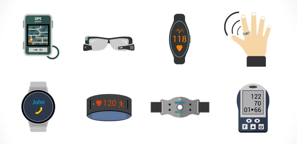
Wearable devices have become a significant application area for electronics. They allow users to monitor health and stay connected without constantly checking smartphones. However, wearable designs present challenges for electronic system designers.
Power and Battery Constraints
The primary design goal for most wearable devices is to keep energy consumption to a minimum. Users dislike frequently charging wearables, especially when they must plug into a power source. Wireless charging offers greater convenience but can increase charging time due to limits on the power that can be transferred to the device.
DC/DC Conversion and Output Filtering
Optimizing the power consumption of wireless devices requires attention at every design level, including the power path that supplies the electronics. In almost all cases wearables use switching DC/DC converters. Batteries provide a nominal voltage that typically falls as stored charge is depleted.
Many DC/DC converters use a combination of inductors and capacitors on the load side to smooth voltage and current peaks. This is especially important for converters that employ energy-saving pulse-skip modes. Pulse-skip is commonly used during low-activity periods as an alternative to pulse-width modulation (PWM) regulation used when the load is fully active.
Load Transients and Output Impedance
Load transients tend to produce spikes due to the impedance of the equivalent series inductance (ESL) and the high-frequency behavior of output capacitors. Recovery from load-step transients can cause overshoot or undershoot depending on the direction of the transient. Reducing the impact of supply voltage error relies on the energy stored in the output capacitors and the converter's response time. For reliable regulation, it is important to have wide loop bandwidth in the DC/DC converter, low equivalent series resistance (ESR) in the output capacitors, and sufficient output capacitance for energy storage.
The ability to maintain efficient, low-noise output under load changes depends on how much overshoot and undershoot the regulator will tolerate and how much ripple voltage appears at the switching frequency. Peak overshoot and undershoot are roughly equal to the load-step current multiplied by the impedance of the output capacitor at the loop crossover frequency. Similarly, ripple voltage approximates the output capacitor impedance multiplied by the inductor peak-to-peak current.
Reducing Output Impedance
Increasing inductance reduces the inductor peak-to-peak current, but large inductors can complicate PCB and enclosure design. It is difficult to make high-value inductors in the thin form factors required by wearables. Therefore, focusing on lowering the output capacitor impedance at the relevant switching frequencies is generally more practical. Although capacitor impedance shows a frequency-dependent minimum at its self-resonant frequency, ESR largely controls impedance in many cases.
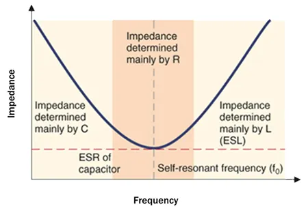
Figure 1: How impedance changes with increasing frequency.
Sources of ESR
While an ideal capacitor stores all energy in the dielectric, real capacitors exhibit some series resistance. ESR usually arises from dielectric losses and the materials used for electrodes and terminals. At low frequencies up to the kilohertz range, dielectric loss is the main contributor to ESR. At higher frequencies, ESR from the electrode and terminal metals dominates. These losses become significant due to skin effect and increase roughly with the square root of frequency.
Manufacturers typically specify ESR in milliohms at selected frequencies, so it is important to consider capacitor ESR performance near the converter switching frequency and loop crossover. Because ESR is frequency-dependent, capacitor ESR performance also matters in RF circuits. RF capability is an important feature for modern wearables. Although protocols such as Bluetooth Low Energy and IEEE 802.15.4 operate at relatively low transmit powers, ESR in RF sections can be a significant part of overall loss.
Capacitor Types for Low ESR
Multilayer ceramic capacitors (MLCCs) tend to have low ESR and ESL but have traditionally been limited by size and capacitance. Electrolytic and tantalum capacitors have provided larger capacitance values but often with higher ESR. Advances in polymer capacitor designs developed to improve tantalum-device reliability have significantly reduced ESR. Polymer dielectrics also avoid ignition issues associated with some tantalum designs, improving safety and performance characteristics.
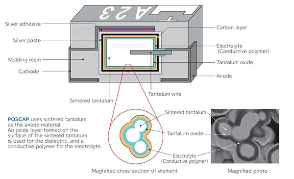
Figure 2: Construction of a low-ESR polymer capacitor.
Panasonic's POSCAP series of polymer electrolyte capacitors can achieve ESR as low as 6 mΩ, with minimum impedance commonly occurring between 100 kHz and 2 MHz. This range fits many efficient DC/DC converter switching frequencies. POSCAP devices use highly conductive polymer electrolytes to lower ESR compared with aluminum electrolytic and tantalum capacitors. Different POSCAP subfamilies trade off frequency-dependent behavior; for example, the TPSF series offers low ESL suited for applications where low impedance at high frequency matters, with minimum impedance near 1 MHz. Compared with ceramic capacitors, POSCAP capacitance is more stable over temperature and exhibits very low voltage bias.
Another advantage of polymer capacitors is the absence of piezoelectric effects. Many MLCC dielectrics are piezoelectric and mechanically expand and contract with charging changes. If a DC/DC converter switches in the audio range, such mechanical vibrations can create audible noise.
MLCCs, Converter Selection, and EMI
MLCCs are widely available, and the trend toward higher switching frequencies allows DC/DC converters to use relatively small output capacitance, enabling their use in wearable power stages. For example, TI's TPS61291 is designed for relatively small output capacitance and needs only a 22 μF output capacitor for a typical 3.3 V rail, delivering up to 100 mA. With a low-power 15 nA static mode, such converters suit low-power wearable applications.
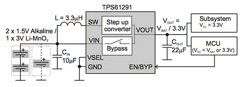
Figure 3: Schematic showing a 22 μF capacitor with the TI TPS61291.
TPS61291 and similar converters can be paired with MLCCs that use X5R or X7R temperature characteristics, such as those from AVX. The series includes X5R devices with capacitances up to 100 μF. Other dielectric types, like Z5U, may not be suitable for power filtering because their capacitance varies significantly with temperature.
The combination of switching power supplies and low-power wireless communications can create EMI issues. Converters generate high-frequency EMI: fast switching creates voltage ringing. RC damping networks are often placed in parallel at the converter input to suppress noise and protect semiconductor components. Because MLCCs are optimized for low ESR, EMI suppression circuits typically require added resistance to maintain sufficient impedance for effective damping. This can undesirably reduce power efficiency, sometimes by as much as 4%, which is significant for battery-life-sensitive devices.
An alternative is to use noise-absorption capacitors such as TDK's YNA series. YNA devices are designed with higher ESR so they can suppress excessive ringing when used at the DC/DC converter input without requiring additional series resistance.
ESR from MLCCs decreases as capacitance increases because conductor resistance falls with more internal electrode layers. YNA construction allows ESR to be raised above its nominal value by combining different internal electrode patterns.
Conclusion
Wearable devices have driven renewed attention to low-power design techniques. Using capacitors with controlled ESR in and around DC/DC converter circuits can help improve energy efficiency and extend battery life.