ALLPCB


Introduction
When people think of Huawei, they often think of mobile phones, but the company is also a traditional equipment manufacturer. Its main products are communication systems, including data transmission equipment, data communications, broadband multimedia equipment, power equipment, and wireless communication devices. These systems mainly serve carriers and government/enterprise networks, i.e. B2B business. Consumer mobile phones are only one part of its business.
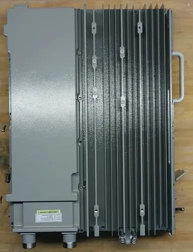
How is a Huawei base station designed? What chips does it use? How is the PCB circuit structured? To answer these questions, we disassembled the Huawei RRU3908, an outdoor radio unit. Each RF front end delivers 20/40 W output power.
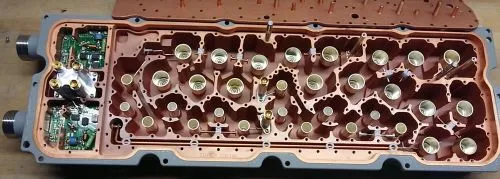
The duplexer appears to be an iris-coupled cavity filter with some inter-cavity coupling. Input and output coupling use a T configuration, connecting to the resonator rather than a coupling loop. Frequency tuning is done by trimmer capacitors. The filter is a wideband band-pass; seeing the filter response would provide more detail.
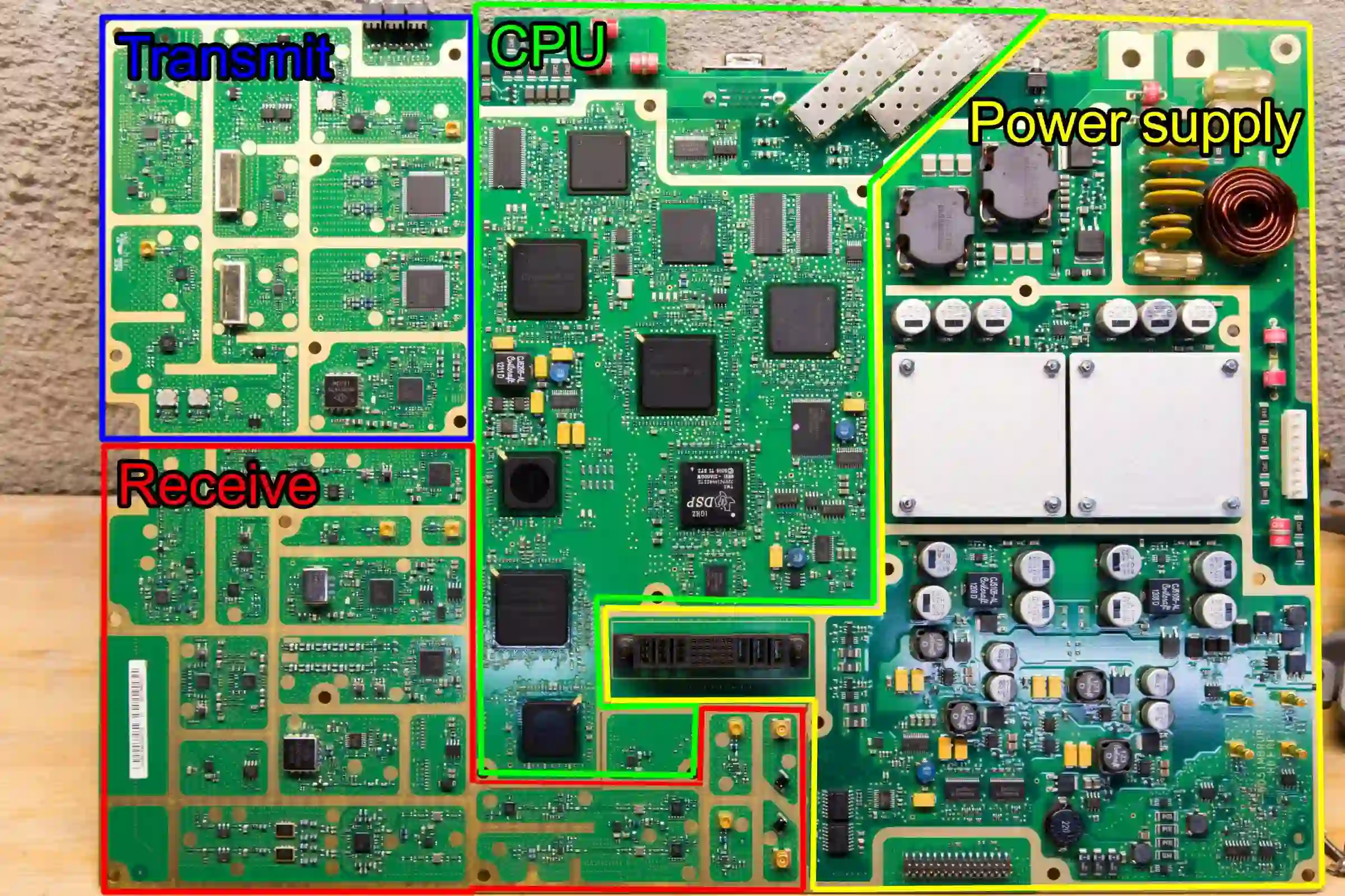
Central Processing Unit
Network communication is handled by a Freescale MPC8321 PowerQUICC II CPU running at 200 MHz, with 2x 256 MB Hynix DDR2 RAM. A PMC QuadPHY 10 Gb controller provides two optical I/O interfaces.
Signal Reception
Input signals arrive on two out-of-phase lines. They are first processed by Skyworks SKY73021-11 1.7–2.2 GHz downconversion mixers, producing frequencies from 2.2 GHz down to 550 MHz. The mixer local oscillator is an Analog Devices ADF4110B. A SAW filter is used for isolation.
Depending on the signal source or type, an Analog Devices AD8376 variable gain amplifier is used before splitting the signal into 3G ADC and 4G ADC paths.
The 3G path analog-to-digital conversion is performed by an Analog Devices AD6655-10, a 14-bit 150 MSPS ADC designed for 3G base stations.
The 4G path includes components such as bidirectional HSWA+1110 RF switches, a dual-channel MAX2039E downconversion mixer, and an Analog Devices AD9230-11 200 MSPS ADC.
All timing is provided by an Analog Devices AD9516-3, a 14-output clock generator with a built-in 2 GHz local oscillator.
Signal Transmission
Single-bit data from an Altera Cyclone III FPGA is processed by two Analog Devices TxDAC AD9788 devices, specified for 16-bit 800 MSPS operation.
Upconversion to the RF carrier is handled by two Analog Devices ADL5375-05 upconverters, covering roughly 400 MHz to 6 GHz. The upconverted signal then passes through a five-stage ceramic resonator band-pass filter.
Signal phase can be adjusted and switched using transistor/EMC techniques and an HPJ2F hybrid coupler.
Before the power amplifiers, a Freescale MMG3004NT1 high-linearity preamplifier provides approximately 17 dB gain from 400 MHz to 2.2 GHz.
To control output level, an MCL 31R5 digital step attenuator is placed before the output connector. This attenuator provides 31.5 dB of attenuation in 0.5 dB steps via a 6-bit serial-control interface.
Power Amplifier
The power amplifier uses a two-stage design. The first stage employs an Infineon PTMA180402FL 40 W RF LDMOS device. Outputs are fed through a Xinger II XC1900A-03S hybrid coupler, which provides two 90-degree phase-shifted signals to the output-stage devices, NXP BLF6G20LS-140 140 W RF LDMOS transistors.
Outputs are recombined in the Xinger II XC1900A-03S hybrid coupler, then routed through a circulator into the duplexer.