ALLPCB


In the world of printed circuit board (PCB) design, reducing costs during optimization is a top priority for engineers and manufacturers. The key to achieving this lies in strategic approaches like layer reduction, careful component selection, and effective thermal management. By focusing on these areas, you can significantly cut expenses without sacrificing performance or reliability. In this comprehensive guide, we’ll dive deep into actionable strategies for cost reduction during PCB optimization, tailored for engineers looking to balance budget and quality.
Why Cost Optimization Matters in PCB Design
Cost optimization in PCB design isn’t just about saving money—it’s about staying competitive in a fast-paced industry. Whether you’re working on consumer electronics, automotive systems, or industrial equipment, every dollar saved can improve profit margins or allow for reinvestment in innovation. The challenge lies in reducing costs while maintaining signal integrity, thermal performance, and overall durability. Let’s explore how layer reduction, component selection, and thermal management can help achieve this balance.
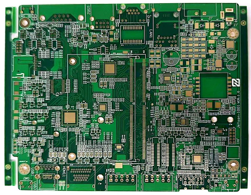
Strategy 1: Layer Reduction for Cost Savings
One of the most direct ways to reduce costs in PCB design is by minimizing the number of layers in your board. Each additional layer increases manufacturing complexity, material usage, and overall production expenses. Here’s how to approach layer reduction effectively.
Evaluate the Need for Multiple Layers
Start by analyzing your design requirements. Do you really need a 6-layer or 8-layer board? For simpler circuits, a 2-layer or 4-layer design might suffice. For instance, if your project doesn’t involve high-speed signals (above 100 MHz) or complex routing, reducing layers can save up to 20-30% on fabrication costs. Use design software to simulate signal paths and ensure that a reduced layer count won’t compromise performance.
Optimize Routing Efficiency
Efficient routing can often eliminate the need for extra layers. Focus on placing components strategically to shorten trace lengths and avoid crossovers. By doing so, you can fit more connections into fewer layers. For example, grouping high-speed components closer together can reduce the need for additional signal planes, cutting both cost and potential signal interference.
Balance Cost with Performance
While reducing layers saves money, it’s critical to maintain performance. If your design involves impedance-controlled traces (e.g., 50 ohms for high-speed signals), ensure that the remaining layers can support proper grounding and power distribution. A poorly planned layer reduction can lead to electromagnetic interference (EMI) or signal degradation, costing more in redesigns than the initial savings.
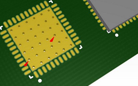
Strategy 2: Smart Component Selection to Lower Expenses
The components you choose directly impact both the cost and performance of your PCB. By making informed decisions during component selection, you can achieve significant savings without compromising quality.
Opt for Standard Components
Custom or specialized components often come with a high price tag and longer lead times. Instead, prioritize standard, widely available components that meet your design needs. For example, choosing a standard 0402 resistor over a custom size can reduce costs by up to 10-15% per unit, especially in high-volume production. Check component libraries for alternatives that offer similar performance at a lower cost.
Bulk Purchasing and Supplier Relationships
Buying components in bulk can lead to substantial discounts. Work closely with suppliers to negotiate pricing for large orders or long-term contracts. Additionally, selecting components from a single supplier can reduce shipping costs and simplify logistics. For instance, sourcing capacitors, resistors, and ICs from one vendor might save 5-10% compared to multiple sources.
Minimize Component Count
Reducing the total number of components on your board cuts costs in materials and assembly. Review your schematic for opportunities to combine functions into a single IC or eliminate unnecessary parts. For example, using a multi-channel op-amp instead of multiple single-channel ones can reduce both component count and board space, saving on manufacturing and assembly expenses.

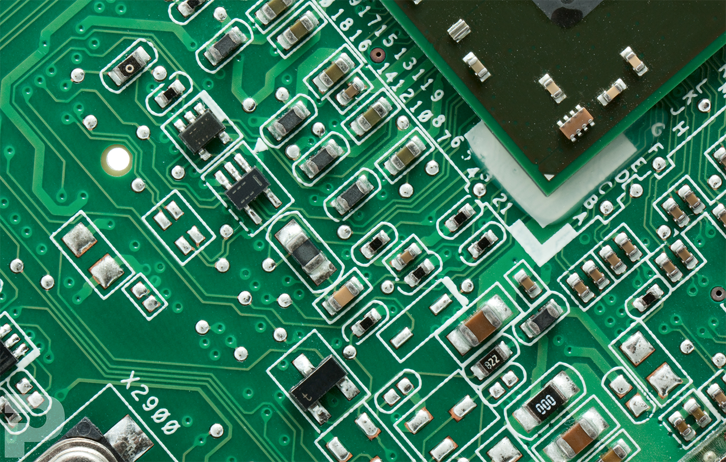
Strategy 3: Effective Thermal Management for Long-Term Savings
Thermal management is often overlooked in cost optimization, but poor heat dissipation can lead to component failure, reduced lifespan, and costly repairs. By designing for thermal efficiency, you save money on maintenance and replacements while ensuring reliability.
Use Thermal Vias for Heat Dissipation
Thermal vias are small, plated-through holes that transfer heat from hot components to other layers or a heat sink. Placing thermal vias under high-power components like voltage regulators or microcontrollers can reduce operating temperatures by 10-15°C. This approach minimizes the need for expensive cooling solutions like external heat sinks, which can cost $2-5 per unit in bulk.
Optimize Component Placement for Heat Distribution
Place heat-generating components away from sensitive parts and ensure proper spacing for airflow. For example, positioning a power IC near the edge of the board allows better heat dissipation compared to placing it in the center. Simulation tools can help predict hot spots and guide placement, preventing thermal issues that could lead to redesign costs.
Select Materials with Thermal Performance in Mind
The choice of PCB material impacts both cost and thermal management. Standard FR-4 material is cost-effective for most designs but may not handle high temperatures well. For high-power applications, consider materials with better thermal conductivity, like metal-core PCBs, though they are pricier. Balance the upfront cost with long-term reliability to avoid failures that could cost 2-3 times more in repairs or replacements.
Additional Tips for Cost Optimization in PCB Design
Beyond layer reduction, component selection, and thermal management, consider these additional strategies to further reduce expenses during optimization.
Design for Manufacturability (DFM)
Adhering to DFM guidelines ensures your design is easy to produce, reducing fabrication errors and costs. For example, maintaining a minimum trace width of 6 mils and spacing of 6 mils can prevent manufacturing issues that lead to scrapped boards. Many design tools offer DFM checks to catch potential problems early, saving up to 15% on production costs.
Leverage Simulation Tools
Simulation software can identify issues like signal integrity problems or thermal hot spots before production. Investing time in simulation can save thousands of dollars by avoiding costly prototypes. For instance, running a thermal simulation to ensure a component operates below 85°C can prevent premature failure and warranty claims.
Plan for Scalability
Design with future production volumes in mind. A design optimized for low-volume prototyping might not be cost-effective at scale. For high-volume runs, panelization—arranging multiple PCBs on a single panel—can reduce fabrication costs by 10-20%. Work with your manufacturer to optimize panel layouts for maximum yield.
Balancing Cost and Quality in PCB Optimization
While cutting costs is essential, it’s equally important to maintain the quality and reliability of your PCB. A design that’s too focused on savings might fail under real-world conditions, leading to higher expenses in the long run. Always prioritize critical performance metrics like signal integrity (e.g., maintaining impedance within ±10% of target values) and thermal thresholds (e.g., keeping junction temperatures below 125°C for most ICs). Use the strategies discussed—layer reduction, component selection, and thermal management—as tools to achieve a cost-effective yet robust design.
Conclusion: Start Optimizing for Cost Today
Reducing costs during PCB optimization is a multi-faceted process that requires careful planning and execution. By focusing on layer reduction, smart component selection, and effective thermal management, you can achieve significant savings without compromising on performance. Start by evaluating your current design for opportunities to simplify layers, choose cost-effective parts, and improve heat dissipation. With these strategies in hand, you’re well-equipped to create high-quality PCBs that meet both budget and technical requirements.
Implementing these cost-saving measures not only benefits your bottom line but also positions you as a forward-thinking engineer in a competitive field. Take the first step today by reviewing your PCB design with these principles in mind, and watch as efficiency and savings go hand in hand.