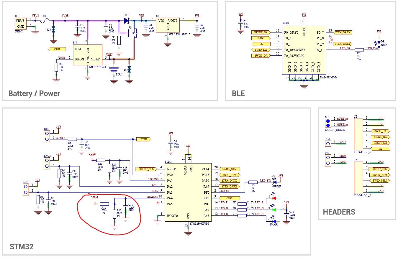
ALLPCB


When developers seek maximum performance from an algorithm and software techniques are exhausted, hardware/software repartitioning can be used to accelerate the workload. FPGAs make it straightforward to exchange software modules for hardware modules without changing the processor or performing board-level modifications. This article explains how to use FPGAs to implement hardware acceleration for algorithms.
To extract maximum performance from code, typical approaches include algorithmic optimization, using lookup tables instead of computations, matching native word sizes, using register variables, unrolling loops, or writing assembly. If these techniques are insufficient, options include moving to a faster processor, changing processor architecture, or parallelizing across multiple processors. Another practical option is to convert timing-critical code sections to hardware functions that can run 5–100x faster. Modern programmable logic enables this approach.
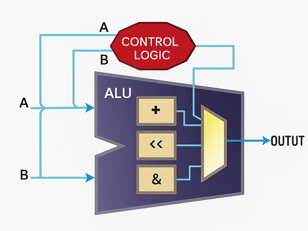
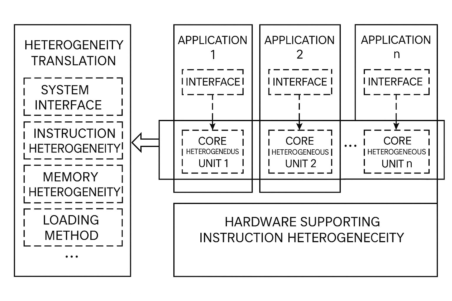
Figure 1: Configurable processor architecture with custom instructions.
Introduction to FPGA-based Hardware Acceleration
Low-cost programmable logic is increasingly used in embedded systems, giving designers a way to increase performance without major changes to the processor or board. Programmable logic can convert compute-intensive functions into hardware accelerators. From the software perspective, this is simply offloading a function call to a custom hardware module, which often runs far faster than the same code optimized in assembly or replaced by a lookup table.
1. What Is Hardware Acceleration
Hardware acceleration uses hardware modules to replace software algorithms and exploit inherent hardware speed. From the software viewpoint, the interface to a hardware accelerator is like calling a function; the difference is the function resides in hardware and is transparent to the caller.
Depending on the algorithm, execution time can improve by up to two orders of magnitude. Hardware is much faster for certain operations, such as complex math, bulk data movement, and repetitive transformations. Later sections discuss common software operations that benefit significantly from hardware acceleration.
When a system uses an FPGA, custom hardware can be added at any point in the development cycle. Designers can develop software immediately and run on hardware parts before finalization. An incremental approach can determine which portions should be implemented in hardware versus software. Vendor development tools support seamless switching between hardware and software, generating HDL for bus and interrupt logic and producing tailored software libraries and include files for the system.
2. RISC with Some CISC Capabilities
One RISC goal is to keep instructions simple so they execute very fast. CISC architectures take the opposite approach: instructions may execute less quickly but accomplish more per instruction. Both styles are widely used and have merits.
Combining RISC simplicity and speed with selected CISC-like complex operations implemented in hardware can be advantageous. This is essentially what hardware acceleration does: adding application-specific hardware modules increases processing capability and reduces code complexity and density by replacing software with hardware. In other words, hardware is traded for speed and simplicity.
There are two main ways to implement hardware acceleration: custom instructions and hardware peripherals. Custom instructions are usually added as extensions to the arithmetic logic unit (ALU) of a configurable processor, so the processor treats them like any other instruction with its own opcode. From C code, a macro can be generated so invoking the custom instruction looks like a function call.
If a custom instruction requires several clock cycles to complete but is called continuously, it can be pipelined so that a result is produced every clock cycle after an initial latency.
Alternatively, acceleration can be implemented as a memory-mapped hardware peripheral. In this case, data are written to the peripheral rather than passed to a software function. The computation occurs outside the CPU, allowing the CPU to continue executing while the peripheral works. Unlike custom instructions, a peripheral can access other system peripherals or memory without CPU intervention.
The choice between a custom instruction and a peripheral depends on what the hardware must do, how it must operate, and how long it needs to run. Operations that complete in a few cycles are often better as custom instructions because of lower overhead. Peripherals typically require several instructions to write control, status, and data registers and one instruction to read results. For longer computations, a peripheral is preferable because it does not stall the CPU pipeline. Pipelined custom instructions are another option.
Another distinction is that custom instructions handle a limited number of operands and return a single result; the operand set varies by instruction set architecture. If the hardware must read or write memory or other peripherals, a memory-mapped peripheral is required because custom instructions cannot access the bus directly.
Figure

Figure 2: Hardware core implementing a 16-bit CRC algorithm.
3. Selecting Code for Hardware Acceleration
To optimize C code for speed requirements, run profiling tools or inspect the code to find hotspots. Familiarity with the codebase helps identify bottlenecks.
Even after finding a bottleneck, optimization can be challenging. Techniques include using native word-size variables, precomputed lookup tables, and standard software algorithm optimizations. These can yield several-fold speedups. Writing critical sections in assembly used to provide substantial gains, but modern compilers are often very effective, limiting the benefit of hand-coded assembly. For substantial improvements, software optimizations may not suffice.
Hardware implementations can be orders of magnitude faster than software. Therefore, do not convert entire modules blindly; instead choose operations that run particularly well in hardware, such as bulk data moves, heavy arithmetic, and frequently repeated loops. If a task consists of several arithmetic operations, consider accelerating the entire task in hardware. Sometimes accelerating just one operation in a task meets performance requirements.
4. Example: Hardware-Accelerating a CRC Algorithm
Checksum algorithms like CRC are good candidates for hardware acceleration due to repetitive, compute-intensive operations. The following example walks through optimizing a CRC algorithm and options for hardware implementation.
Start with conventional software optimizations, then move to a custom instruction for further acceleration. This section compares performance and trade-offs of different implementations.
CRC is used to detect data corruption during transmission. CRC algorithms are popular because they offer high error-detection capability without much impact on throughput; CRC bits are appended to the data. CRC computation involves modulo-2 division by a 16- or 32-bit polynomial, implemented via iterative XORs and shifts. For a 16-bit polynomial, processing a byte can require hundreds of instructions, so for large messages the instruction count grows into the tens of thousands. Any optimization significantly improves throughput.
The function in Listing 1 takes a pointer to the message and the byte count and returns the CRC remainder. Although the input is in bytes, the computation is bitwise, so the algorithm is inefficient because AND, shift, XOR, and loop control are performed bit by bit.
Listing 1: Bitwise CRC algorithm in C.
/** The width of the CRC calculation and result.* * Modify the typedef for a 16 or 32-bit CRC standard.*/ typedef unsigned char crc; #define WIDTH (8 * sizeof(crc)) #define TOPBIT (1 << (WIDTH - 1)) crc crcSlow(unsigned char const message[], int nBytes){ crc remainder = 0; /* * Perform modulo-2 division, a byte at a time. */ for (int byte = 0; byte < nBytes; ++byte) { /* * Bring the next byte into the remainder. */ remainder ^= (message[byte] << (WIDTH - 8)); /* * Perform modulo-2 division, a bit at a time. */ for (unsigned char bit = 8; bit > 0; bit--) { /* * Try to divide the current data bit. */ if (remainder & TOPBIT) { remainder = (remainder << 1) ^ POLYNOMIAL; } else { remainder = (remainder << 1); } } } /* * The final remainder is the CRC result. */ return (remainder); }
4.1 Software Optimizations Using a Lookup Table
Use software techniques to optimize the CRC. Because the polynomial divisor is constant, all possible byte-width CRC results can be precomputed and stored in a lookup table. Processing then proceeds byte by byte with a single table lookup per byte.
The table values can be stored in ROM or RAM, initialized before the CRC calculation. The table contains 256 entries, one for each possible 8-bit value. Listing 2 shows C code that initializes the table and uses it.
crc crcTable[256]; void crcInit(void){ crc remainder; /* * Compute the remainder of each possible dividend. */ for (int dividend = 0; dividend < 256; ++dividend) { /* * Start with the dividend followed by zeros. */ remainder = dividend << (WIDTH - 8); /* * Perform modulo-2 division, a bit at a time. */ for (unsigned char bit = 8; bit > 0; bit--) { /* * Try to divide the current data bit. */ if (remainder & TOPBIT) { remainder = (remainder << 1) ^ POLYNOMIAL; } else { remainder = (remainder << 1); } } /* * Store the result into the table. */ crcTable[dividend] = remainder; } } /* crcInit() */ crc crcFast(unsigned char const message[], int nBytes){ unsigned char data; crc remainder = 0; /* * Divide the message by the polynomial, a byte at a time. */ for (int byte = 0; byte < nBytes; ++byte) { data = message[byte] ^ (remainder >> (WIDTH - 8)); remainder = crcTable[data] ^ (remainder << 8); } /* * The final remainder is the CRC. */ return (remainder); } /* crcFast() */
This reduces computation to a loop where each byte uses two XORs, two shifts, and two loads. The lookup table trades memory for speed and yields about a 9.9x improvement over bitwise calculation. If more performance is needed, larger tables or hand-written assembly may help, but for 20x–500x improvements hardware acceleration is required.
4.2 Custom Instruction Implementation
A CRC algorithm consists of repeated XOR and shift operations that are simple to implement in hardware. Because such a hardware module can compute CRC in a few cycles, implementing CRC as a custom instruction is often preferable to a peripheral, provided no other system peripherals or memory access are required.
When implemented in hardware, the algorithm should process 16- or 32-bit chunks depending on the CRC standard. For CRC-CCITT (16-bit polynomial), processing 16 bits at a time is ideal. On an 8-bit microcontroller, overhead to load operands and return results reduces efficiency. Figure 2 shows a hardware core that shifts message bits into the XOR/shift hardware one bit at a time for a 16-bit implementation.
Listing 3 shows C examples that compute CRC over a 64 KB data block, targeting a configurable embedded processor.
unsigned short crcCompute(unsigned short *data_block, unsigned int nWords){ unsigned short* pointer; unsigned short word; /* * initialize crc reg to 0xFFFF */ word = nm_crc (0xFFFF, 1); /* nm_crc() is the CRC custom instruction */ /* * calculate CRC on block of data * nm_crc() is the CRC custom instruction * */ for (pointer = data_block; pointer < (data_block + nWords); pointer ++) word = nm_crc(*pointer, 0) return (word); } int main(void){ #define data_block_begin (na_onchip_memory) #define data_block_end (na_onchip_memory + 0xffff) unsigned short crc_result; unsigned int data_block_length = (unsigned short *)data_block_end - (unsigned short *)data_block_begin + 1; crc_result = crcCompute((unsigned short *)data_block_begin, data_block_length); }
With a custom instruction, CRC computation in code appears as a function call or macro. For example, on the Nios processor the build tools generate a macro nm_crc() to invoke the custom instruction. The CRC register inside the custom instruction must be initialized according to the CRC standard. The loop then invokes the custom instruction once per 16-bit word. This approach can be about 27x faster than the bitwise implementation.
4.3 Peripheral + DMA Implementation
Implementing CRC as a memory-mapped peripheral and using DMA to feed data to it can achieve even higher throughput. DMA removes the additional cycles the CPU would spend loading operands for each CRC computation. While the peripheral processes one CRC chunk, DMA can present the next chunk. Figure 3 shows a system block diagram with a CRC peripheral and DMA.
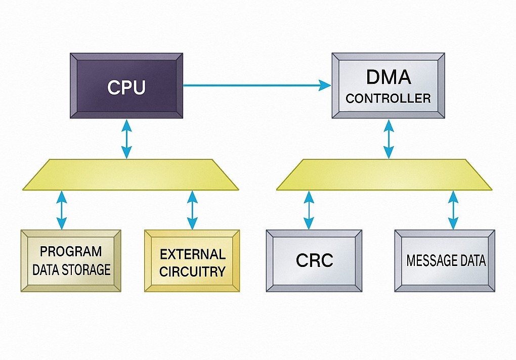
Figure 3: System block diagram showing a CRC peripheral and DMA.
On a 64 KB data block, a custom peripheral with DMA can be about 500x faster than pure software bitwise CRC. Performance gains from DMA increase with larger data blocks because DMA setup overhead is small relative to its high transfer rate. For small data lengths, DMA may not be worthwhile.
The implementations discussed here for CRC-CCITT (16-bit polynomial) were realized on a Nios processor inside an Altera Stratix FPGA. Performance comparisons across data sizes and approximate FPGA resource usage (memory or logic cells) illustrate that more hardware resources generally yield higher speed. This is a trade of hardware resources for performance.
5. Advantages of FPGA-based Acceleration
With FPGA-based embedded systems, designers do not have to decide early on which modules must be hardware vs software. If extra performance is required mid-design, FPGA logic can accelerate hotspots. Programmable logic can be tailored to the application so only required hardware is used without board-level changes, provided FPGA capacity is sufficient. Designers do not have to switch processors or write assembly to achieve higher performance.
Using a configurable processor within an FPGA gives design flexibility. Each software module can be implemented as a custom instruction or as a hardware peripheral. Adding custom hardware can yield higher performance than off-the-shelf microprocessors.
FPGAs provide abundant resources that configurable processor systems can exploit.
Algorithms can be implemented in software or hardware. For convenience and cost, most operations remain in software unless higher speed is required. Software optimization helps, but sometimes it is insufficient. In such cases, hardware acceleration is an effective option.
FPGAs simplify exchanging software and hardware modules without changing the processor or performing board-level modifications. Designers can balance speed, logic, memory, code size, and cost. FPGAs enable custom embedded systems that add functionality and optimize performance.