ALLPCB


Introduction
In the artificial intelligence era, electronic robots are being integrated into industry, services, and healthcare at an accelerating pace. From precision tasks in manufacturing to assistance in medical diagnostics, from efficient logistics to in-home service, robots have increased productivity and improved quality of life.
As applications expand, sensitivity to electrostatic discharge (ESD) has become a more prominent issue. This stems from increasing technical complexity, diverse operating environments, and dynamic operational requirements. The following discusses the common ESD-related problems and circuit design measures to mitigate them.
ESD Problems Encountered by Robots
Damage to electronic components: ESD can permanently damage semiconductor components inside robots, such as integrated circuits and chips. When electrostatic voltage exceeds a component's threshold, dielectric layers can break down, rendering the device inoperative.
Data corruption: Static can interfere with storage elements, causing data errors or loss. For example, static discharge can alter program code stored in flash memory, affecting control logic and runtime behavior.
System faults: ESD events can cause control system malfunctions, abnormal robot motions, or communication interruptions. Static may disturb sensor signal transmission, degrading environmental perception and impacting navigation and operation.
Electromagnetic interference: Electrostatic fields and discharges can interfere with radio-frequency circuits and wireless modules, reducing communication quality or causing dropouts. For instance, static can disrupt wireless charging signals, affecting charging efficiency and stability.
Circuit Design Measures for ESD
With increasing precision of microcontrollers and other components, circuit-level ESD protection becomes critical. While manufacturing controls can reduce ESD risk, field environments cannot be tightly controlled. Robust circuit design practices are therefore essential. The following methods can effectively reduce ESD-related problems in electronic robots.
Reasonable Layout and Routing
PCB layout and routing play a key role in ESD resilience. The main recommendations are:
- Logical segregation: Separate circuits that generate ESD or high interference from ESD-sensitive circuits. For example, place power and driver circuits apart from control and sensor circuits to minimize interference coupling.
- Layering principles: In multilayer boards, place power and ground planes adjacent to each other to use the capacitance between them, creating low-impedance return paths and reducing charge accumulation on the board.
- Control trace spacing: Maintain adequate spacing between signal and power traces. Avoid routing sensitive signal traces parallel to high-voltage or high-current lines to reduce electromagnetic coupling.
- Shorten traces: Minimize the length of high-frequency and sensitive traces to reduce opportunities for ESD coupling. For example, keep microprocessor clock trace lengths as short as possible to lower the risk of clock signal distortion from ESD.
ESD Protection Circuits
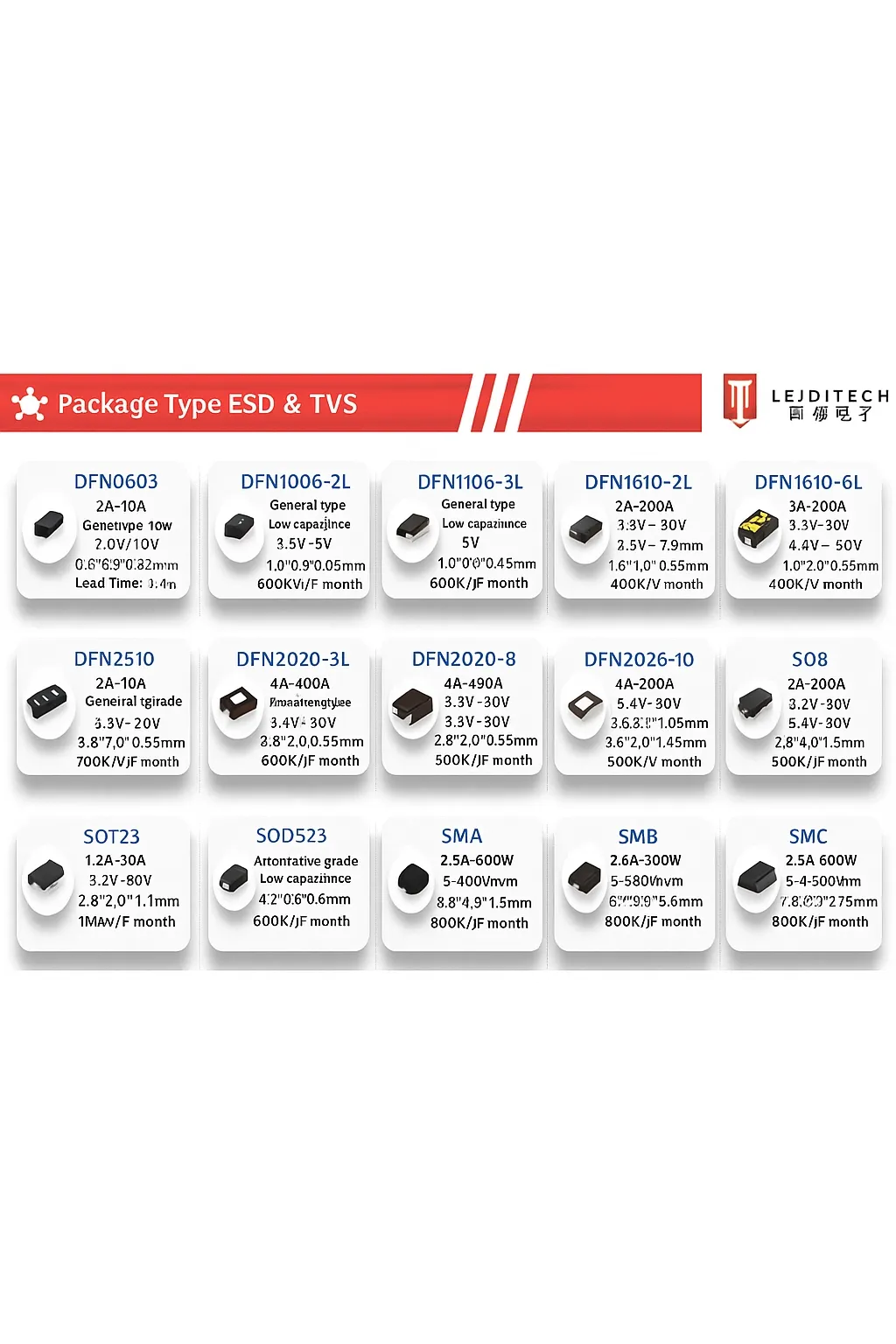
TVS diode protection: Place transient voltage suppression (TVS) diodes across critical signal and power lines. Design ESD protection around sensitive ICs with RC filtering and clamp diodes. When a transient high voltage occurs, TVS diodes respond rapidly to clamp the voltage at a safe level, protecting other components. For example, installing TVS diodes on communication interfaces helps prevent ESD damage to communication chips.
Sensor and Interface Circuit Design
Sensor protection: Add ESD protection circuits at sensor I/O ports, for example using TVS diodes to limit port voltages to safe ranges. For sensors sensitive to static, such as capacitive sensors, provide grounded shielding around the sensor to reduce external static interference.
Interface optimization: Integrate dedicated ESD protection devices on external interfaces like USB and HDMI. These devices rapidly dissipate ESD energy, protecting interface circuits and connected internal electronics. For network and power interfaces, use isolation transformers, optocouplers, and common-mode filtering to prevent external static from entering internal circuitry.
Filtering and Decoupling
Power filtering: At power inputs, design LC or pi filters to use inductors and capacitors to remove high-frequency noise and static pulses, providing stable power rails for circuit modules. For example, series inductors combined with bulk capacitors to ground can suppress ESD-induced disturbances on supply lines.
Decoupling capacitor placement: Place multiple decoupling capacitors of different values close to each IC's power pins, typically 0.1 μF for high-frequency noise and 10 μF for low-frequency disturbances and charge storage. Proper decoupling helps maintain stable power and prevents ESD-induced supply transients from affecting chips.
Grounding and Shielding
Single-point grounding: Use a single-point grounding approach where internal circuit module grounds are tied to a common reference point. This reduces ground potential differences and minimizes static circulating currents.
Ground conductor design: Ensure ground traces and planes have adequate width and low resistance so static charges can be quickly and effectively conducted to chassis or earth ground. Design ground widths according to expected current levels to minimize ground resistance.
Electromagnetic shielding: For circuits susceptible to static disturbance, such as RF and audio modules, use metal shields that are properly grounded. Shields block external electrostatic fields and prevent internal charge radiation, improving ESD immunity.
Use of shielded cables: For sensitive signal transmission, use shielded cables. For example, encoder signal lines and camera video cables with grounded outer shields reduce static interference and help preserve signal integrity.