ALLPCB


As defect levels and process variability attract increasing attention, DRAM manufacturers continue to seek cost-effective screening and process-improvement solutions. The introduction of faster interfaces and multi-chip packages makes meeting these needs more challenging.
DRAM in modern systems
Dynamic random-access memory plays a central role across many electronic systems, from phones and personal computers to automotive ECUs and hyperscale data center servers. It is also a key component in AI/ML systems, where the volume of data to be processed and stored is rapidly increasing. Memory products now span a wide range, from low-cost parts to high-capacity DRAMs with faster read/write transactions.
DRAM faces unique challenges. Although it has traditionally been low cost, quality and reliability requirements have risen, particularly for safety- and mission-critical applications. Shrinking bit cells increase sensitivity to defects and process variability. While built-in repair and error-correcting code (ECC) can mitigate some manufacturing defects, engineering teams still rely heavily on inspection and electrical testing.
Expectations for quality and RAS (reliability, availability, and serviceability) vary by application. Data rates and interfaces differ widely depending on the volume and speed of transfers between memory and processors. High-bandwidth memory (HBM) interfaces add complexity by enabling migration from PCB and DIMM slots to 2.5D and 3D packaging.
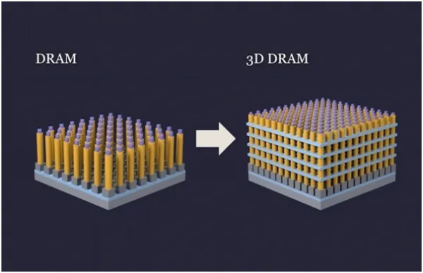
Related Reading: 3D DRAM Roadmap and Production Timeline
Wafer inspection and process control
Yield improvements for new DRAM technologies are most effective when meaningful data are captured at process steps closest to where defects and variability occur. Yield, process, and device engineers rely on wafer-level inspections to screen defects and provide feedback on process variability. They also correlate process variation or defects with bit-map failures from wafers to measure key device electrical parameters during wafer manufacture.
Increased defectivity is a direct consequence of shrinking DRAM cells. Modern DRAM technologies use buried wordline structures with stacked capacitors to reduce short-channel effects. Numerous manufacturing defects can affect DRAM performance, and these are routinely tested. Examples include contamination during etch, particles that hinder lithography or etch, wafer contamination that allows mobile ions such as copper to migrate and alter retention time, and process variation that changes isolation-layer thickness and thus capacitor coupling. Crystalline defects in the wafer lattice can cause temporary or permanent leakage in DRAM cell mechanisms.
Higher sampling rates, up to 100%, help detect defects earlier. This is especially important in industries such as automotive, where customer quality requirements can drive very high inspection rates.
Sampling strategy depends on the wafer or assembly process step and the intended purpose. For front-end post-lithography inspection, 100% sampling may not be required if the goal is monitoring process drift, particularly for mature nodes. For shipment quality assurance, however, 100% sampling is often mandatory to decide wafer or die acceptance based on defect limits.
Device and yield engineers use electrical testing early in the FEOL to gain insight into process variation. Parametric tests measure electrical characteristics such as threshold voltage, on/off current, and capacitance. As DRAM process nodes advance and NAND stacking increases, margins on critical storage elements shrink, making electrical process-control monitoring of these basic elements increasingly important. Typical parametric testing occurs after transistor-layer formation and after contact pad formation near the end of line.
After wafer test, yield engineers use bit-map data from failed DRAM cells to localize potential defect sources. The bit-map is a rasterized aggregation of pass/fail results from all tests.
Built-in self-test (BiST) remains the fundamental method for generating cell-level memory results that correlate inline defects with device impact. Combined with bit-map pattern classifiers, BiST helps device engineers understand cell sensitivity under stress.
Manufacturing test requirements
DRAM testing occurs at wafer probe and package test. The final assembled package, target system requirements, and cost considerations drive the overall test flow, including ATE requirements and the scope of tests.
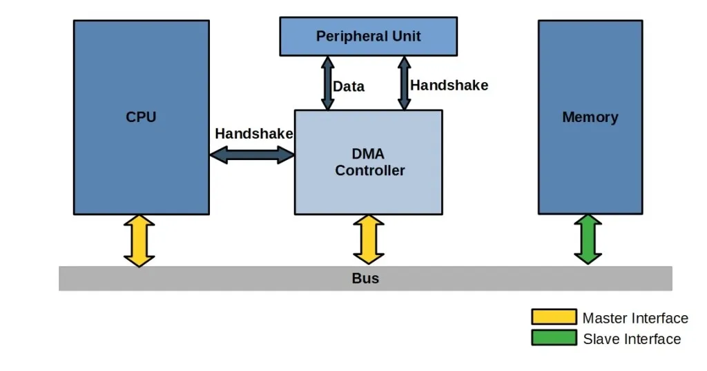
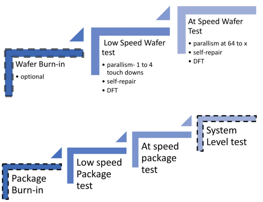
Engineers use two insertions to manage long test times for large DRAM arrays and to address high-speed interface requirements. In the first insertion, memory test algorithms are applied at lower speeds. In the second insertion, a known-good die (KGD) or companion chip uses high-speed interfaces and runs the memory test algorithms at operational speed. Both insertions are performed during wafer test and can be repeated at package test.
Wafer tests are typically run at relatively low frequencies, around 100 MHz, to identify weak cells that can then be repaired. For cost reasons, high parallelism is required, achieved by probing each die multiple times per handler touchdown. This requires probe cards with many thousands of pins and substantial mechanical load. KGD testing requires higher-speed arrays and full-speed backend tests, which are performed with lower parallelism high-speed probe cards; for that reason, KGD usually does not support the highest speed grades.
Burn-in can be used to accelerate discovery of reliability-related defects by applying high temperature and high voltage while switching circuit signals. There are wafer-level and package-level burn-in systems, and in some cases system-level testing can be used to exercise actual workloads.
Wafer-level test and burn-in (WLTBI) allow memory suppliers to stress all die on a wafer to identify marginal and failing cells, enabling removal of infant-mortality die and improving multi-chip and heterogeneous module yield. Modules are constructed using several technologies, such as processors, memory, and silicon photonics, each with different voltage, timing, and temperature stress requirements that must be applied at the wafer level for the specific technology. Increased density and frequency place growing demands on wafer thermal dissipation during WLTBI, driving requirements for higher-performance systems.
What makes memory different
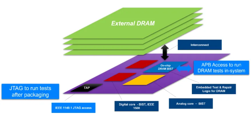
Memory ATE systems differ from logic ATE in several respects. First, they require pattern generation and on-chip repair functionality.
Memory ATE solutions must include an algorithmic pattern generator (APG) and failure-capture memory to store failure information and access. For wafer sort, memory repair failure analysis is essential and provides critical process feedback. Online repair analysis is compute intensive and requires significant ATE hardware accessibility.
The second major difference is high-speed interfaces. For SoC devices that include memory controllers, high-speed I/O faults can be addressed with integrated DFT features, allowing SoC testers to avoid being limited by memory I/O rates. Memory testers still must perform full-rate testing to guarantee that parts operate at speed, including highly demanding timing tests. Memory ATE must also support extremely high test-point counts to offset the long test times of large memories. This forces ATE designers to develop highly integrated test electronics to meet high-speed capabilities, and new memory standards drive demand for new test equipment, shortening equipment lifecycles.
DRAM test patterns cover a wide address range and include specific memory tests for refresh behavior, cell leakage, and a long list of repair-oriented patterns. Many tests require data dependence from adjacent bit cells. For example, the row-hammer test emphasizes a cell's ability to retain data after repeated reads. High-speed tests separately validate memory performance and interface performance, checking operational timing specifications (such as tAC, tRCD) and I/O timing specifications (such as tVB, tVA).
DRAM requires extensive internal test modes, often proprietary, to achieve high parallelism during test, for example by compressing multiple I/Os into one, or by modifying timing parameters beyond normal operating limits to find weak cells.
Although some wafer defect/failure mechanisms resemble those in logic technologies, reliable bit storage demands additional attention. High density increases defect sensitivity. If every failed bit, row, or column were considered a hard fail, yields would be very low. This reality led designers to include spare rows and columns and in-test repair mechanisms. At the wafer level, repair can be done with laser or electrically blown fuses; at the package level, only e-fuse repair is available. ECC can manage unit failures during manufacturing test and in-system operation. Die area devoted to repair structures can be 5% to 10% of total area.
To reduce cost, parallel testing is used at both die and package test. Memory is a commodity, so testing cost dominates. DRAM uses extreme parallelism. For wafer test, trends move toward one-touchdown (1TD) handling. Achieving 1TD requires assembling many pin electronics and power supplies for ATE. Innovations that integrate ATE and processors into compact units can increase parallelism per footprint.
Test design for testability (DFT) is essential for DRAM. A programmable memory test engine enables running extensive memory algorithms and allows engineering teams to trade test time for coverage at each stage of the device lifecycle. As an IP block, memory BiST must support various DRAM I/O interfaces, whether LPDDR, DDR, GDDR, or HBM, each with different latency, data rate, and protocol requirements. Other DFT solutions support burn-in test insertion and allow parallel testing using I/O compression. DFT can also alter internal DRAM timing to find weak cells and supports array repair and HBM channel repair.
DRAM repair principally follows manufacturing test standards. Over the past decade, JEDEC defined post-package repair (PPR), providing one row of repair per die. Standardized approaches allow repairs at boot time.
Historically, programmable test engines were seldom exposed to end users, but this is changing as reliability and field-serviceability requirements rise. With longer lifetimes, in-field DRAM replacement in servers can be extremely costly. DRAM vendors now provide system-available redundancy, known as post-package repair, standardized by JEDEC. System manufacturers increasingly seek to deploy these solutions in their SoCs to utilize spare capacity in DRAM and improve field reliability.
Related Reading: Understanding Why DRAM Requires Refreshing
DRAM challenges in multi-chip packages
Whether connected to a compute SoC in a 2.5D package or stacked as HBM in a 3D package, DRAM in multi-chip modules presents additional challenges beyond single-die DRAM components. Some challenges are unique to DRAM, others are general to multi-chip packaging.
Shrinking pad pitch and large numbers of microbumps create inspection and test challenges. Multi-chip products require additional 2D/3D inspection and metrology. Additional interconnect steps such as fan-out, microbump, and direct bonding add process steps that must be inspected. Fan-out requires defect inspection for fractured or bridged RDL lines. Microbumps require CD and height metrology plus detection of residual defects on top of bumps. Direct bonding requires inspection for cracks, voids, and delamination.
HBM delivers much higher data rates at lower power and is implemented as a wide interface for 2.5D and 3D packaging. The small microbump pitch and numerous connections among stacked die make channel repair options necessary to accommodate bad bonds between die. As stack depth increases, so does the multiplicative risk. This requires test strategies to detect failing channels and enable channel repair, an area where DFT is critical. However, inspection methods can produce higher false-positive rates for potential bonding defects due to poor metallurgical contact.
Through-silicon vias (TSVs) and microbump interconnects enable stacked HBM die. As part of the known-good-die flow, test processes typically screen for defective TSVs before die thinning. After bonding the stacked die, they are inspected and tested. Inspection plays an important role in assessing solder quality, die alignment (overlap), and die warpage.
Currently, copper pillars with solder caps are common. As pitch decreases, the industry will gradually transition toward hybrid bonding. For vertical stacks, die placement accuracy is critical for monitoring and maintaining bond integrity. Excessive misplacement can stretch or break bumps, leading to dewetting. Bond-line thickness (BLT) compression is also important: excessive BLT causes dewetting, small BLT can cause solder extrusion, and in some cases solder may be entirely extruded off the pad area.
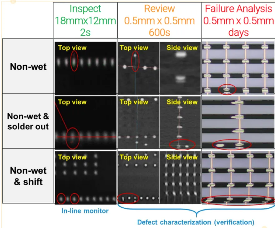
Hard shorts and open failures are easiest to isolate. Partial or edge bonds raise concerns because not all bonds may be detected, and some connections can fail in the field. Detailed inspection helps but is challenging.
Tools that can operate at sufficient speed and sensitively distinguish layers and assess bond-impacting attributes are currently limited, particularly for 8-, 12-, or 16-layer stacks. As die become thinner, warpage and alignment become significant issues that require monitoring.
Integrating DRAM into multi-chip modules raises the bar for test and DFT.
Multi-chip modules introduce additional testability, accessibility, and multi-die diagnostic challenges. HBM adds complications because logic die and memory die cannot be tested independently; their interconnect must be tested together. For such die stacks, access mechanisms such as IEEE 1500 are necessary. Diagnostics must distinguish and isolate failures for physical failure analysis. A DRAM-based test engine typically resides on the logic die, between the controller and the PHY on the master chip. In test modes it controls the PHY to execute read/write commands to test external memory and interconnects.

For multi-chip component manufacturing, traceability is key to enabling operational feedback and die performance matching. Ensuring that module-level performance aligns with other die types in the package and monitoring version control are essential. For example, placing slower memory die in a high-performance package can degrade the entire module, lowering average selling price and profitability. Another risk is placing memory with reduced dynamic operating range into a package expected to operate across wide environmental variance.
Summary
Many view DRAM as a commodity for cost reasons, but treating all DRAM the same is misleading. Memory performance is critical to the overall performance of some of the most complex computing systems.
As compute systems demand more exabyte-scale data handling and faster execution, DRAM migration toward denser cells and stacked die increases the complexity of testing and inspection. That complexity will continue to grow as faster memories and more complex packages become standard.