 ALLPCB


When it comes to creating a reliable PCB, through-hole technology (THT) remains a trusted choice for many engineers due to its durability and strength. If you're searching for ways to ensure through-hole design reliability and build a robust through-hole design, you're in the right place. This blog will guide you through the best practices for designing through-hole PCBs that stand the test of time, focusing on practical tips and proven strategies.
In the sections below, we’ll dive deep into the essentials of through-hole PCB design, from understanding its benefits to mastering key design rules, optimizing for manufacturability, and ensuring long-term reliability. Whether you're a seasoned designer or just starting, these insights will help you create boards that perform consistently under stress.
Why Choose Through-Hole Technology for Reliability?
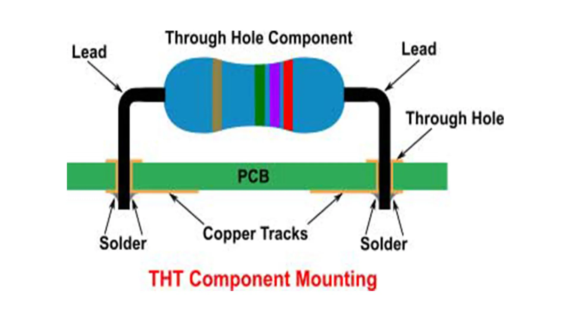
Through-hole technology involves inserting component leads into drilled holes on a printed circuit board (PCB) and soldering them in place. This method offers unmatched mechanical strength compared to surface-mount technology (SMT), making it ideal for applications where durability is critical. Think of industries like aerospace, automotive, and industrial equipment—sectors where a reliable PCB can mean the difference between success and failure.
Here are a few reasons why through-hole design is synonymous with reliability:
- Strong Mechanical Bonds: Soldered leads create robust connections that resist vibration and mechanical stress, ensuring a robust through-hole design.
- High Power Handling: THT components can handle higher current and voltage levels, which is crucial for power electronics.
- Ease of Repair: Through-hole components are easier to replace or rework, extending the lifespan of the PCB.
Key Principles of Through-Hole Design Reliability
To achieve a reliable PCB with through-hole technology, you need to focus on several core design principles. These guidelines ensure that your board not only functions well but also withstands environmental and operational challenges.
1. Optimize Hole and Pad Sizes for Strength
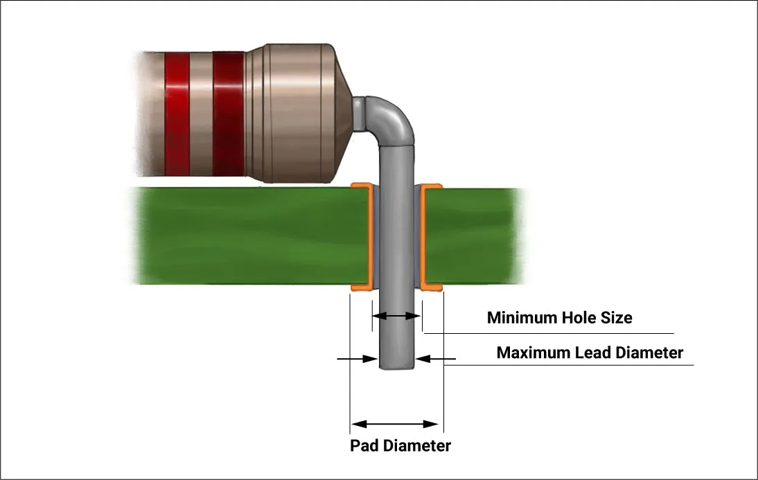
The size of the drilled holes and surrounding pads (annular rings) plays a significant role in through-hole design reliability. If the hole is too small, inserting components becomes difficult, leading to potential damage. If it’s too large, the solder joint may be weak.
Follow these standards for optimal design:
- Hole Diameter: The hole should be 0.2 mm to 0.3 mm larger than the component lead diameter to allow easy insertion while ensuring a snug fit.
- Annular Ring Width: Maintain a minimum annular ring width of 0.25 mm around the hole to provide enough area for solder to form a strong joint.
- IPC Standards: Adhere to IPC-2221 guidelines, which recommend specific hole-to-pad ratios for different component types to ensure durability.
By carefully calculating these dimensions, you create a foundation for a robust through-hole design that minimizes the risk of joint failure.
2. Ensure Proper Component Spacing
Crowding components on a PCB can lead to issues like heat buildup and soldering defects, both of which harm reliability. Proper spacing is essential for a reliable PCB.
Consider these spacing tips:
- Component-to-Component Distance: Keep at least 2 mm between through-hole components to avoid interference during soldering.
- Hole-to-Hole Spacing: Maintain a minimum of 1.5 mm between drilled holes to prevent structural weakening of the board.
- Edge Clearance: Leave at least 3 mm of clearance from the board edge to any hole to avoid cracks or damage during handling.
These spacing rules help reduce stress on the PCB and improve long-term performance.
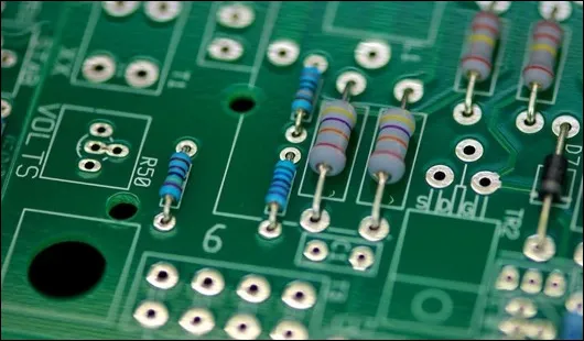
3. Focus on Solder Joint Quality
The solder joint is the heart of a through-hole connection. Poor soldering can lead to cracks, cold joints, or complete failure, undermining through-hole design reliability.
To ensure high-quality solder joints:
- Use Adequate Solder: Ensure the solder fills at least 75% of the hole height for a strong mechanical bond.
- Control Soldering Temperature: Maintain a soldering temperature between 260°C and 300°C to avoid thermal damage to components or the board.
- Inspect Joints: After soldering, inspect for a shiny, smooth finish—a sign of a good joint. Dull or grainy joints may indicate poor adhesion.
High-quality solder joints are a cornerstone of a robust through-hole design.
Designing for Manufacturability (DFM) in Through-Hole PCBs
A reliable PCB isn’t just about how it performs—it’s also about how easily it can be manufactured. Designing with manufacturability in mind reduces errors and ensures consistency during production.
1. Standardize Hole Sizes
Using a variety of hole sizes can complicate the drilling process and increase costs. Stick to a limited set of standard hole sizes (e.g., 0.8 mm, 1.0 mm, 1.2 mm) to simplify manufacturing and maintain through-hole design reliability.
2. Avoid Overloading the Board
Overloading a PCB with too many through-hole components can strain the board’s structure. Balance the use of THT with SMT where possible, especially for smaller components, to reduce the number of holes and maintain board integrity.
3. Provide Clear Documentation
Clear design files and documentation help manufacturers understand your intent. Include detailed notes on hole sizes, component placement, and soldering requirements. This minimizes miscommunication and supports a robust through-hole design.
Enhancing Reliability with Material and Environmental Considerations
The materials you choose and the environment your PCB operates in have a huge impact on its reliability. Let’s explore how to address these factors for a reliable PCB.
1. Select the Right Board Material
The PCB substrate material must withstand thermal and mechanical stress. For through-hole designs, consider:
- FR-4: A common, cost-effective material with good thermal stability (Tg of 130°C to 140°C) for most applications.
- High-Tg Materials: For high-temperature environments, use materials with a Tg above 170°C to prevent delamination during soldering.
Choosing the right material ensures your board remains stable, supporting through-hole design reliability.
2. Account for Thermal Expansion
Thermal expansion can cause stress on solder joints and through-hole connections. Match the coefficient of thermal expansion (CTE) of the PCB material and components as closely as possible. For example, a typical FR-4 board has a CTE of about 14-17 ppm/°C in the X-Y direction, so select components with similar values to minimize strain.
3. Protect Against Environmental Factors
Moisture, dust, and chemicals can degrade a PCB over time. Use conformal coatings to shield the board from these elements. Additionally, ensure that plated-through holes (PTH) are properly finished with a corrosion-resistant material like tin-lead or immersion gold to maintain conductivity.
Testing and Validation for Long-Term Reliability
Even the best designs need to be tested to confirm their reliability. Rigorous testing helps identify weaknesses before they become failures in the field, ensuring a robust through-hole design.
1. Perform Thermal Cycling Tests
Subject your PCB to thermal cycling (e.g., -40°C to 85°C for 1000 cycles) to simulate real-world temperature changes. This test checks for solder joint cracks and material fatigue, critical for through-hole design reliability.
2. Conduct Vibration Testing
For applications in harsh environments, vibration testing (e.g., 10 Hz to 2000 Hz at 5g acceleration) ensures that through-hole connections withstand mechanical stress without loosening.
3. Use Electrical Testing
Verify the integrity of connections with in-circuit testing (ICT) or flying probe testing. These methods detect open circuits, shorts, or poor solder joints, confirming the board’s reliability.
Common Pitfalls to Avoid in Through-Hole PCB Design
Even small mistakes can compromise a reliable PCB. Watch out for these common issues:
- Insufficient Annular Ring: A too-small annular ring can lead to weak solder joints. Always meet the minimum width requirements.
- Poor Lead Preparation: Bent or damaged leads can cause insertion issues, leading to unreliable connections.
- Overheating During Soldering: Excessive heat can damage components or lift pads, so monitor soldering conditions closely.
By avoiding these pitfalls, you’ll be well on your way to creating a robust through-hole design.
Conclusion: Building Reliable PCBs with Through-Hole Technology
Designing a reliable PCB using through-hole technology is all about attention to detail. From optimizing hole and pad sizes to ensuring high-quality solder joints, considering manufacturability, and testing rigorously, each step contributes to through-hole design reliability. By following these best practices, you can create a robust through-hole design that performs consistently, even in the most demanding applications.
Through-hole technology may be traditional, but its strength and durability make it a go-to choice for engineers who prioritize reliability. With careful planning and execution, your PCB designs will not only meet but exceed expectations, delivering long-lasting performance.


