 ALLPCB


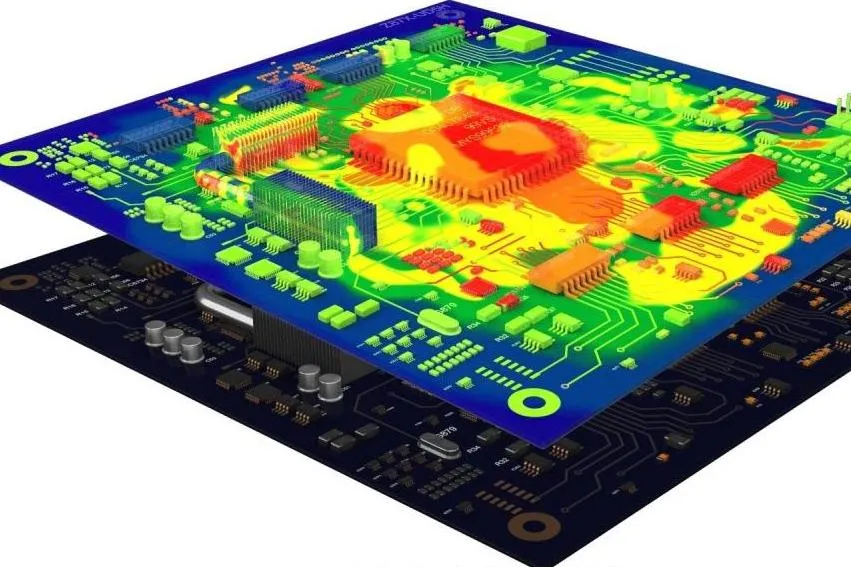
In the fast-evolving world of electronics, high-density PCBs (Printed Circuit Boards) are at the heart of compact, powerful devices. But with smaller footprints and tighter component packing come significant challenges, especially in thermal management. Overheating can degrade performance, damage components, and shorten the lifespan of a device. So, how can engineers tackle the toughest thermal issues in high-density PCBs? The answer lies in strategic design techniques like using thermal vias, minimizing hotspots in HDI (High-Density Interconnect) PCBs, conducting thorough thermal analysis of multi-layered PCBs, and adopting advanced cooling solutions for dense PCBs.
In this comprehensive guide, we’ll dive deep into these critical topics, offering practical solutions and insights to help engineers and designers overcome thermal challenges. Whether you're working on consumer electronics, automotive systems, or industrial applications, mastering thermal management is key to ensuring reliability and performance. Let’s break it down step by step.
Why Thermal Management Matters in High-Density PCBs
High-density PCBs are designed to pack more functionality into smaller spaces. They often feature multiple layers, fine-pitch components, and complex routing, as seen in HDI PCBs. While this allows for incredible innovation, it also generates significant heat in a confined area. Without proper thermal management, this heat can lead to:
- Component failure due to excessive temperatures (often exceeding 85°C for many ICs).
- Signal integrity issues caused by thermal expansion and stress.
- Reduced lifespan of the PCB, with solder joints and materials degrading over time.
Effective thermal management ensures that heat is dissipated efficiently, maintaining optimal operating conditions. By addressing challenges like hotspots and heat buildup in multi-layered designs, engineers can create reliable and long-lasting products.
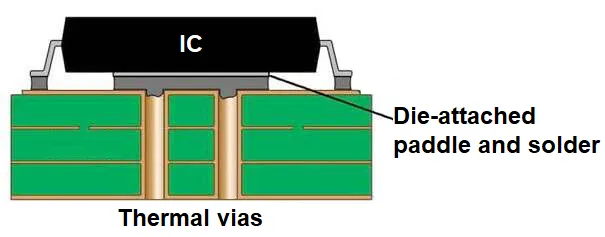
High-Density PCB Thermal Vias: A Core Solution for Heat Dissipation
One of the most effective ways to manage heat in high-density PCBs is through the use of thermal vias. These are small, plated holes that connect different layers of the PCB, allowing heat to transfer from hot components to cooler areas or external heat sinks. Thermal vias act like tiny heat pipes, pulling heat away from critical components.
Here’s how they work and why they’re essential:
- Heat Transfer: Thermal vias are typically placed directly under or near high-power components like processors or power regulators. They transfer heat from the top layer to inner copper planes or the bottom layer, where it can be dissipated.
- Design Considerations: For optimal performance, use a grid of vias (e.g., 0.3 mm diameter vias spaced 1.2 mm apart) under heat-generating components. Studies suggest that a via density of 25-30 vias per square inch can reduce temperatures by up to 10-15°C in high-power areas.
- Material Impact: Filling vias with thermally conductive materials like copper or epoxy can enhance heat transfer by up to 20% compared to unfilled vias.
However, thermal vias must be balanced with electrical design needs. Too many vias can interfere with signal routing or create parasitic capacitance. Advanced PCB design tools can help simulate heat flow and optimize via placement for both thermal and electrical performance.
Minimizing Hotspots in HDI PCBs: Strategies for Even Heat Distribution
HDI PCBs, with their ultra-fine traces and microvias, are prone to localized hotspots due to densely packed components and limited airflow. Hotspots can cause thermal stress, leading to warping or delamination of the board. Minimizing hotspots in HDI PCBs requires a multi-faceted approach.
1. Strategic Component Placement
Place high-power components away from each other to avoid concentrated heat buildup. Use thermal simulation tools to identify potential hotspots during the design phase. For instance, spacing power ICs at least 5-10 mm apart can reduce peak temperatures by 5-8°C.
2. Copper Planes for Heat Spreading
Incorporate large copper planes or pours in the PCB layout to act as heat spreaders. Copper has a thermal conductivity of approximately 400 W/m·K, making it an excellent material for distributing heat evenly across the board. A solid copper plane on an inner layer can reduce hotspot temperatures by up to 10°C in dense designs.
3. Thermal Pads and Underfill
Use thermal interface materials (TIMs) like thermal pads or underfill between components and the PCB. These materials improve heat transfer to the board or heat sink, reducing localized temperature spikes by as much as 15% in some cases.
By combining these techniques, engineers can achieve a more uniform temperature profile across HDI PCBs, preventing damage and ensuring consistent performance.
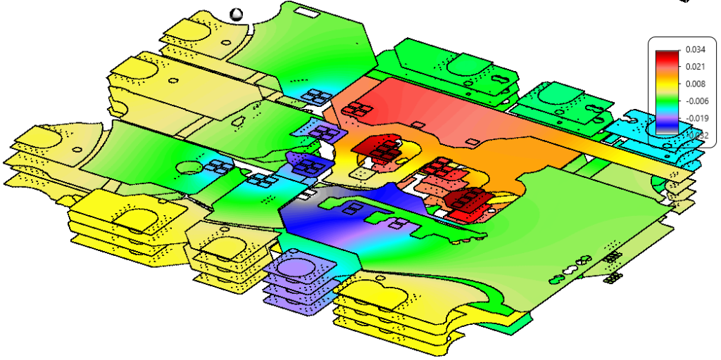
Thermal Analysis of Multi-Layered PCBs: Tools and Techniques
Multi-layered PCBs are common in high-density designs, often featuring 6, 8, or even 12+ layers to accommodate complex circuits. However, the stacked structure traps heat, making thermal analysis of multi-layered PCBs critical to identifying and resolving issues before production.
Why Thermal Analysis Matters
Heat in multi-layered PCBs doesn’t just stay on the surface; it spreads through layers, affecting components and signal integrity. Without analysis, hidden hotspots in inner layers can go undetected until failure occurs. Thermal analysis helps predict temperature distribution and guides design improvements.
Key Tools for Thermal Analysis
- Simulation Software: Tools like ANSYS or Altium’s thermal simulation modules can model heat flow in 3D, accounting for material properties (e.g., FR-4 with a thermal conductivity of 0.3 W/m·K) and component power dissipation (e.g., a 5W power IC).
- Infrared Imaging: Post-production, infrared cameras can map temperature profiles with precision, identifying areas exceeding safe limits (e.g., above 100°C for most components).
Practical Steps in Analysis
- Define power dissipation for each component (e.g., a CPU dissipating 3W).
- Input material properties and stack-up details into simulation software.
- Run simulations to identify peak temperatures and heat flow paths.
- Adjust design elements like via placement or copper thickness (e.g., increasing from 1 oz to 2 oz copper can lower temperatures by 5°C).
Thermal analysis of multi-layered PCBs ensures that heat is managed across all layers, preventing failures and optimizing performance in high-density applications.
Advanced Cooling Solutions for Dense PCBs: Beyond the Basics
While thermal vias and copper planes are effective, extremely dense PCBs often require advanced cooling solutions to handle high heat loads. These cutting-edge techniques can significantly enhance thermal performance in demanding applications like 5G devices or automotive electronics.
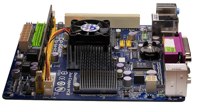
1. Heat Sinks and Active Cooling
Attach heat sinks directly to high-power components to dissipate heat into the surrounding environment. For even better results, pair heat sinks with small fans for active cooling. A heat sink with a thermal resistance of 2°C/W can lower component temperatures by 20-30°C under high load (e.g., 10W dissipation).
2. Vapor Chambers and Heat Pipes
For ultra-dense designs, vapor chambers or heat pipes offer superior heat transfer. These devices use phase-change cooling to move heat away from components at rates far exceeding traditional methods. A vapor chamber can achieve effective thermal conductivity of over 10,000 W/m·K, compared to copper’s 400 W/m·K.
3. Insulated Metal Substrate (IMS) PCBs
IMS PCBs replace traditional FR-4 with a metal base layer (often aluminum) for exceptional thermal performance. With thermal conductivity up to 8 W/m·K, IMS boards are ideal for high-power applications like LED lighting or motor drives, reducing temperatures by 15-25°C compared to standard materials.
4. Liquid Cooling Integration
In extreme cases, liquid cooling systems can be integrated into PCB designs. Microchannels or cold plates near high-heat areas circulate coolant, achieving heat dissipation rates unattainable with air cooling. Liquid cooling can handle power densities exceeding 100 W/cm2, making it suitable for cutting-edge servers or GPUs.
These advanced cooling solutions for dense PCBs provide engineers with powerful tools to tackle the most challenging thermal problems, ensuring reliability even in the most compact and high-performance designs.
Best Practices for Designing Thermally Efficient High-Density PCBs
To wrap up, here are some actionable best practices for managing heat in high-density PCBs:
- Start with thermal simulation early in the design process to catch issues before prototyping.
- Use a combination of thermal vias, copper planes, and interface materials to spread and dissipate heat.
- Opt for advanced cooling solutions like heat sinks or vapor chambers when dealing with power densities above 5 W/cm2.
- Choose materials wisely—consider high-thermal-conductivity laminates or IMS for demanding applications.
- Validate designs with real-world testing, using infrared imaging to confirm simulation results.
By following these guidelines, engineers can create high-density PCBs that perform reliably under even the toughest conditions.
Conclusion: Mastering Thermal Management for High-Density PCBs
Thermal management in high-density PCBs is no longer optional—it’s a critical aspect of modern electronics design. From leveraging high-density PCB thermal vias to minimizing hotspots in HDI PCBs, conducting detailed thermal analysis of multi-layered PCBs, and implementing advanced cooling solutions for dense PCBs, there are numerous strategies to keep temperatures in check. Each approach, whether basic or cutting-edge, plays a vital role in ensuring the performance, reliability, and longevity of electronic devices.
At ALLPCB, we’re committed to supporting engineers with the tools, resources, and expertise needed to solve complex challenges like thermal management. By applying the techniques discussed in this guide, you can design PCBs that not only meet but exceed performance expectations, no matter how dense or demanding the application.


