 ALLPCB


Introduction
Flexible printed circuit boards (PCBs) have become essential in modern electronics, enabling compact designs in devices like wearables, medical sensors, and automotive systems. These boards use bendable substrates to fit into tight spaces, reducing overall assembly weight and volume compared to traditional rigid PCBs. However, flexible PCBs often carry higher production costs due to specialized materials and manufacturing processes. Engineers face the challenge of balancing performance with budget constraints in cost-sensitive projects. This article explores structured strategies for flexible PCB cost reduction, focusing on design choices that maintain reliability while minimizing expenses. By applying these principles, teams can achieve flexible PCB design for cost efficiency without compromising functionality.
What Are Flexible PCBs and Why Cost Optimization Matters
Flexible PCBs consist of conductive traces laminated onto thin, bendable substrates such as polyimide or polyester films, often protected by coverlays instead of soldermasks. Unlike rigid boards, they support dynamic bending, folding, or twisting in applications requiring mechanical flexibility. The relevance stems from growing demand in consumer electronics and IoT devices, where space savings justify the investment. Yet, flexible PCB material cost and manufacturing expenses typically exceed those of rigid boards by factors influenced by substrate choice and complexity. Optimizing design becomes critical for budget-friendly electronics, as even small changes in layout or specs can yield significant savings. Engineers must prioritize design for manufacturability (DFM) early to avoid costly iterations during prototyping.

Key Cost Drivers in Flexible PCB Design and Manufacturing
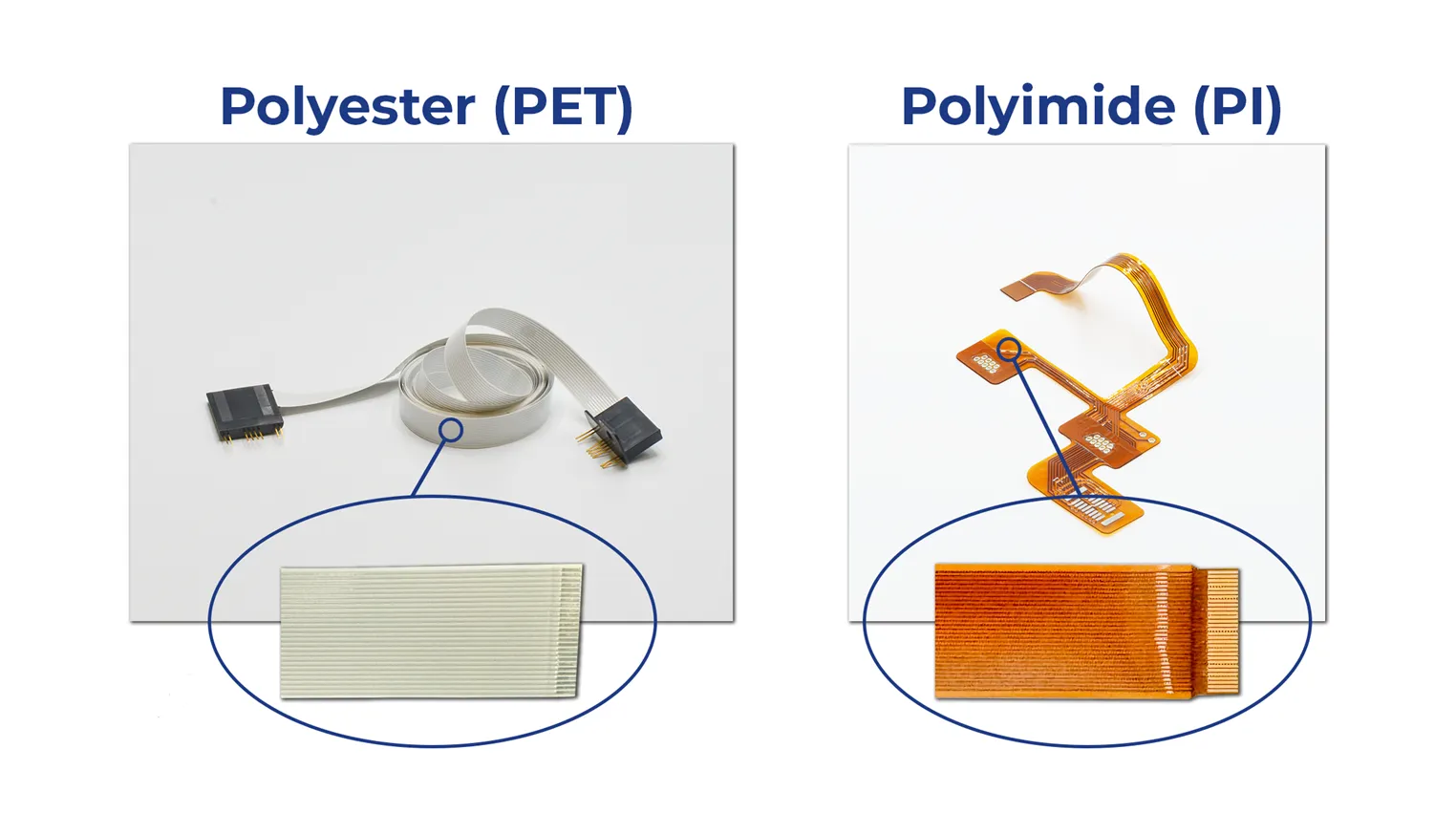
Material selection dominates flexible PCB material cost, with polyimide offering superior thermal stability up to high temperatures but at a premium price compared to polyester. Polyester suits static flex applications where repeated bending is minimal, providing a viable option for flexible PCB cost reduction. Layer count directly impacts expenses, as each additional layer requires more lamination steps and increases material usage. Copper weight and thickness add to costs; thinner foils suffice for low-current signals, reducing raw material needs. Vias, especially blind or buried types, complicate drilling and plating, driving up flexible PCB manufacturing cost. Trace width and spacing tolerances also play a role, with finer features necessitating advanced etching processes that elevate per-unit pricing.
Bend radius requirements further influence production complexity, as tight bends demand precise control to prevent cracking. Coverlay application and stiffener integration add labor and materials if not standardized. Panel utilization efficiency affects yield; inefficient nesting wastes substrate area. Surface finishes like ENIG cost more than HASL but offer better reliability in flex environments. Understanding these drivers allows engineers to target high-impact areas for optimization. Overall, these factors can multiply costs exponentially in multi-layer designs.
Material Selection Strategies for Flexible PCB Cost Savings
Choosing the right substrate is foundational for flexible PCB material cost management. Polyimide excels in dynamic flex with high bend cycles and temperature resistance, but polyester provides adequate performance for one-time folds at a lower price point. Adhesiveless laminates reduce delamination risks while sometimes cutting costs over adhesive-based stacks. Copper foil type matters; rolled annealed copper enhances bend durability over electrodeposited, though at higher initial expense. Coverlay materials should match substrate properties to avoid mismatch stresses. Engineers should evaluate application demands against cost trade-offs during schematic stages.
Standardizing on fewer material variants streamlines procurement and minimizes setup changes in fabrication. For instance, opting for 1 oz copper in signal layers conserves material without sacrificing integrity in many designs. Testing prototypes under IPC-2223 guidelines ensures material choices align with performance needs. This approach not only lowers direct costs but also improves yield rates. Collaborative reviews with manufacturers early can reveal cost-effective alternatives tailored to volume.
Optimizing Stackup and Layer Configuration
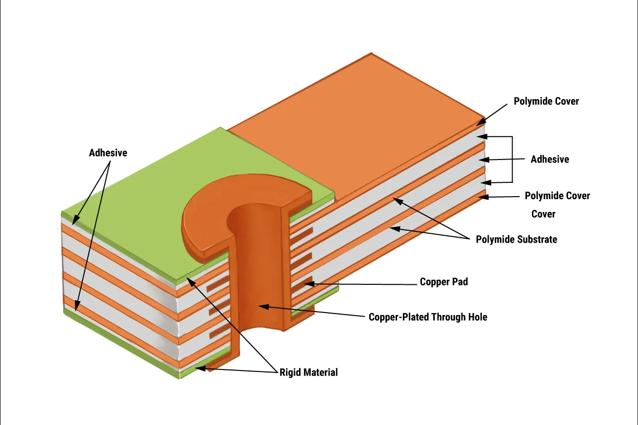
Minimizing layer count stands as a primary tactic in flexible PCB design for cost. Single or double-sided flex often suffices for simple interconnects, avoiding the expense of multi-layer builds. Consolidating signals into fewer layers reduces interlayer vias and registration challenges. Hybrid rigid-flex designs should limit flex sections to essential areas, integrating rigid parts for component mounting. Stackup symmetry prevents warpage, which could otherwise increase scrap rates and costs.
Bend zones require careful planning; isolating flex tails from rigid areas simplifies lamination. Using fill patterns or ground planes judiciously avoids excess copper that inflates etching costs. IPC-6013 qualification specs guide stackup validation for performance under flex stress. Thinner overall profiles enable tighter panel nesting, boosting throughput. These configurations directly contribute to flexible PCB manufacturing cost reductions by shortening process times.
Design Rules and DFM Principles for Cost Control
Adhering to DFM rules prevents expensive rework and yield losses. Maintain minimum bend radii at 10 times the board thickness to avoid trace fractures, aligning with industry practices. Widen traces to 0.15 mm or more where current allows, easing etching tolerances. Prefer through vias over microvias unless density demands otherwise, as the latter require laser drilling. Standardize pad sizes and avoid odd shapes that complicate plating.
Panelization optimizes substrate use; array multiple boards with shared rails for depaneling efficiency. Looser tolerances on non-critical dimensions cut inspection and machining costs. Incorporate fiducials for alignment without custom features. These practices enhance manufacturability, yielding 20-30% savings in prototypes. Regular DFM checks integrate seamlessly into CAD workflows.
Panelization and Production Scaling Techniques
Efficient panelization transforms per-unit costs for volume runs. Nesting algorithms in design software maximize board count per panel, reducing waste. Stepped panel edges accommodate varying flex lengths. V-scoring or tab routing simplifies singulation post-fabrication. For high volumes, full-panel builds amortize setup costs across units.
Tighter process controls in scaling minimize variability, but avoid over-specifying for prototypes. Batch similar designs to share tooling. These techniques amplify flexible PCB cost reduction benefits as quantities increase.
Conclusion
Optimizing flexible PCB design for cost involves holistic decisions across materials, stackup, DFM, and production scaling. Selecting polyester for static apps, minimizing layers, and panelizing efficiently deliver substantial savings. Adhering to standards like IPC-2223 and IPC-6013 ensures reliability alongside affordability. Engineers achieve budget-friendly electronics by prioritizing these strategies from concept through fabrication. The result is flexible, reliable boards that fit project constraints without performance trade-offs.
FAQs
Q1: How can engineers achieve flexible PCB cost reduction through material choices?
A1: Polyester substrates offer a lower-cost alternative to polyimide for static flex applications, where dynamic bending is absent. Evaluate thermal and mechanical needs against budgets; polyester handles up to moderate temperatures effectively. Combine with thinner copper foils for signal layers to further trim expenses. This selection maintains functionality while cutting raw material outlays significantly. Always validate via bend testing per industry guidelines.
Q2: What design practices contribute most to flexible PCB design for cost?
A2: Reduce layer counts to essentials and consolidate routing to minimize vias and lamination steps. Widen traces and standardize bend radii to simplify etching and handling. Implement DFM by avoiding tight tolerances on non-critical features. Panelize arrays efficiently for better yield. These steps lower both prototype and production costs without reliability impacts.
Q3: Why does layer configuration affect flexible PCB manufacturing cost?
A3: More layers demand additional lamination cycles, increasing material use and process time. Multi-layer stacks complicate registration and via formation, raising defect risks. Opt for single or double-sided where possible, isolating flex zones. This reduces handling complexity and boosts panel efficiency. Resulting savings scale with volume.
Q4: How does panelization impact flexible PCB material cost?
A4: Panelization maximizes substrate utilization by nesting multiple boards, minimizing waste scraps. Shared edges and rails streamline depaneling, cutting labor. For flex, account for varying shapes to fit optimally. Higher yields per panel directly lower per-unit material allocation. This technique proves especially effective in medium to high volumes.
References
IPC-2223E — Sectional Design Standard for Flexible/Rigid-Flexible Printed Boards. IPC, 2019
IPC-6013D — Qualification and Performance Specification for Flexible/Rigid-Flexible Printed Boards. IPC, 2014
IPC-9204 — Flex Circuit Assembly Bend Testing and Performance. IPC, 2004


