ALLPCB


Introduction
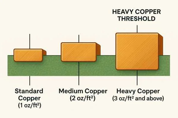
Printed circuit boards rely on copper layers to conduct electricity and manage heat. Standard designs often use 1 oz copper per square foot, yet many applications benefit from thicker traces. Three ounce copper provides approximately three times the cross sectional area of conventional layers. This increase supports higher current loads while maintaining lower resistance. Engineers select this specification when thermal demands or power requirements exceed typical limits. The approach enhances overall board capability without requiring major redesigns in many cases.
What Is 3 oz Copper and Why It Matters
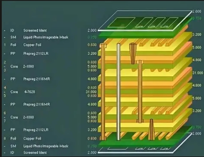
Copper weight describes the thickness of the conductive layer measured in ounces per square foot. One ounce corresponds to roughly 35 micrometers, so three ounces reaches about 105 micrometers. This specification appears in power electronics, motor controllers, and high current distribution networks. Thicker copper improves the ability to carry substantial amperage while limiting temperature rise. It also contributes to mechanical strength of traces during handling and operation. Industry qualification processes such as those outlined in IPC 6012E address performance expectations for rigid boards that incorporate heavier copper weights.
Technical Principles Behind Performance Gains
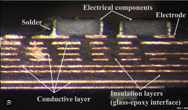
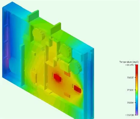
Thicker copper reduces electrical resistance along each trace according to basic Ohm law relationships. Lower resistance directly supports improved PCB signal integrity by minimizing voltage drop and reducing electromagnetic interference in sensitive paths. Heat generated by current flow dissipates more effectively because the greater cross sectional area increases thermal mass and conduction paths. This mechanism enhances PCB thermal performance and helps prevent localized hot spots that could degrade components or laminate materials. Durability improves as well because wider or thicker traces resist mechanical stress and vibration better than thin equivalents. Reliability metrics benefit when boards operate continuously under elevated loads, as the design maintains consistent electrical characteristics over extended periods.
Engineers calculate current carrying capacity using guidelines that account for trace width, copper thickness, and allowable temperature rise. The increased thickness permits narrower traces for the same current rating, which preserves board real estate. Thermal modeling often shows that three ounce designs achieve lower peak temperatures under identical load conditions compared with one ounce layouts. Signal paths carrying high frequency content experience reduced skin effect losses when resistance is lowered by thicker copper. These combined effects make the specification suitable for applications where both power delivery and signal quality must coexist on the same board.
Practical Design and Manufacturing Considerations
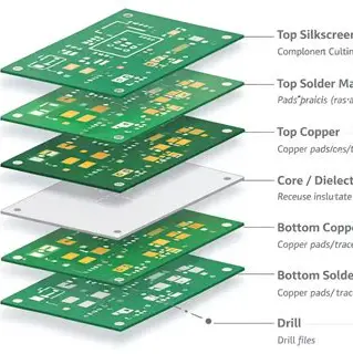
Design teams begin by reviewing current requirements and temperature constraints for each net. They adjust trace widths and copper weights accordingly while maintaining spacing rules for voltage isolation. Thermal vias placed under heat generating components transfer energy into internal planes or heat sinks more efficiently when paired with heavier copper. Fabrication processes accommodate three ounce layers through controlled etching and plating sequences that preserve fine features elsewhere on the board. Assembly steps such as soldering remain compatible provided reflow profiles follow established thermal limits. Quality control checks verify copper thickness and uniformity to ensure the finished board meets performance targets.
Best practices include specifying copper weight on the fabrication drawing with clear callouts for each layer. Engineers often combine three ounce outer layers with one ounce inner layers to balance cost and performance. Testing under load confirms that temperature rise stays within acceptable bounds before final release. When vibration or flexing occurs in the end product, the added copper mass contributes to trace robustness without additional reinforcement. Documentation of these choices supports traceability and future revisions.
Conclusion
Three ounce copper offers measurable improvements in current handling, heat management, and long term stability for demanding PCB applications. The specification integrates into existing design flows with straightforward adjustments to trace geometry and thermal planning. Engineers achieve better PCB signal integrity and PCB thermal performance while supporting overall PCB durability and PCB reliability. Careful application of these principles yields boards that operate reliably under challenging electrical and environmental conditions.
FAQs
Q1: What are the main 3 oz copper PCB advantages for high current designs?
A1: Thicker copper layers provide greater cross sectional area, which lowers resistance and allows higher current without excessive heating. This supports compact layouts while meeting thermal targets. Engineers gain flexibility in trace routing and component placement. The approach also strengthens traces against mechanical stress during assembly and use.
Q2: How does 3 oz copper improve PCB signal integrity in mixed signal boards?
A2: Reduced trace resistance minimizes voltage drop along power and ground paths that serve sensitive analog or digital circuits. Lower impedance helps maintain clean return paths and reduces noise coupling. The thicker conductor also aids heat spreading, which keeps component temperatures stable and preserves signal timing accuracy.
Q3: In what situations does 3 oz copper enhance PCB thermal performance and PCB durability?
A3: Applications with sustained high current or concentrated heat sources benefit from the increased thermal mass and conduction area. Temperature gradients flatten, extending component life and reducing warpage risk. The added copper thickness also improves resistance to vibration and handling damage, contributing to longer service intervals.
Q4: How does heavier copper contribute to overall PCB reliability?
A4: Consistent electrical performance under load reduces the likelihood of intermittent failures or thermal runaway. Mechanical robustness of traces lowers the chance of cracking during thermal cycling. Boards built to recognized qualification standards demonstrate repeatable results across production lots when copper weight is properly specified and controlled.
References
IPC-6012E — Qualification and Performance Specification for Rigid Printed Boards. IPC, 2017
IPC-2152 — Standard for Determining Current Carrying Capacity in Printed Board Design. IPC, 2009
JEDEC J-STD-020E — Moisture/Reflow Sensitivity Classification for Nonhermetic Surface Mount Devices. JEDEC, 2014