ALLPCB


In the fast-paced world of electronics, efficiency and cost-effectiveness are key to staying ahead. One technique that significantly boosts both is panelization in PCB manufacturing. But what exactly are the benefits of panelization, and how does Design for Manufacturability (DFM) play a role in enhancing speed, cutting costs, and improving material utilization? Simply put, panelization groups multiple PCB designs onto a single panel for production, streamlining processes and reducing waste, while DFM ensures designs are optimized for manufacturing ease. In this comprehensive guide, we’ll dive deep into how these strategies impact manufacturing efficiency and deliver measurable results for your projects.
What Is PCB Panelization and Why Does It Matter?
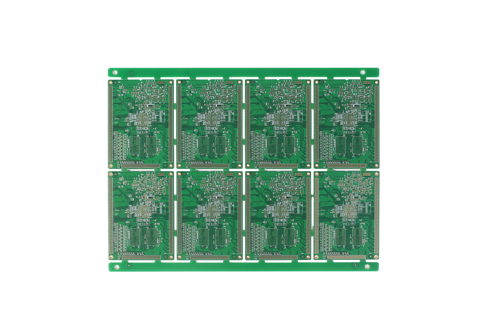
PCB panelization is the process of arranging multiple printed circuit boards (PCBs) onto a larger panel for manufacturing. Instead of producing each board individually, several identical or different designs are grouped together, processed as a single unit, and later separated into individual boards. This approach is a cornerstone of modern electronics production, especially for high-volume runs.
The importance of panelization lies in its ability to optimize every step of the manufacturing process. From fabrication to assembly and testing, handling multiple boards at once reduces time, labor, and material costs. When combined with DFM principles—designing with manufacturing constraints in mind—panelization becomes even more powerful, ensuring fewer errors and faster turnaround times.
Key Benefits of Panelization in PCB Manufacturing
Panelization offers a range of advantages that directly address critical concerns like cost cutting, material utilization, and manufacturing efficiency. Let’s explore these benefits in detail to understand how they impact your bottom line and project timelines.
1. Cost Cutting Through Streamlined Production
One of the most significant panelization benefits is its ability to reduce production costs. By processing multiple boards simultaneously, manufacturers cut down on setup times for machines like pick-and-place systems or stencil printers. For instance, assembling components on a panel of 10 boards in one go can slash assembly time by up to 50% compared to handling each board separately, especially in high-volume production.
Additionally, panelization minimizes labor costs. Workers spend less time handling individual boards, and automated systems can operate more efficiently with larger panels. This reduction in manual intervention also lowers the risk of human error, saving money on potential rework or scrap.
2. Enhanced Material Utilization for Reduced Waste
Material waste is a major cost driver in PCB manufacturing. Standard laminate sheets often come in sizes like 18 x 24 inches or 21 x 24 inches. When producing small or irregularly shaped boards individually, a lot of material can go unused. Panelization maximizes material utilization by fitting as many boards as possible onto these standard sheets, cutting scrap rates significantly.
For example, in high-volume production scenarios, optimized panel layouts have been shown to increase board yield by up to 20%. This means more usable boards per panel and substantial savings on raw materials like copper-clad laminates. Efficient material use also aligns with sustainable practices, reducing environmental impact—a growing priority in the industry.
3. Boosted Manufacturing Efficiency with Automation Compatibility
Manufacturing efficiency is at the heart of panelization’s value. Panels are designed to be compatible with automated equipment, such as reflow ovens, stencil printers, and testing machines. This compatibility speeds up every stage of production. For instance, a pick-and-place machine can populate components across an entire panel in a single pass, rather than resetting for each individual board.
Panels also provide structural stability, especially for smaller boards that are prone to damage or misalignment during handling. A stable panel reduces the likelihood of defects during soldering or testing, ensuring consistent quality and faster throughput. In some cases, panelization can reduce lead times by days, depending on the complexity and volume of the order.
4. Improved Quality Control and Testing
Testing individual boards can be time-consuming and error-prone, especially for small designs. Panelization allows for batch testing, where multiple boards are evaluated at once using automated optical inspection (AOI) or in-circuit testing (ICT). This not only speeds up the quality assurance process but also ensures uniformity across the batch, as all boards on a panel experience the same manufacturing conditions.
By catching defects early at the panel level, manufacturers can avoid costly rework on individual units. This streamlined approach to quality control is a direct result of thoughtful panel design and contributes to overall project efficiency.
How Design for Manufacturability (DFM) Enhances Panelization
While panelization offers clear advantages, its effectiveness depends heavily on how well the PCB is designed for manufacturing. DFM is the practice of creating designs that align with manufacturing capabilities and constraints, minimizing errors and maximizing efficiency. When applied to panelization, DFM can take the benefits of cost cutting and manufacturing efficiency to the next level.
1. Optimizing Panel Layouts with DFM
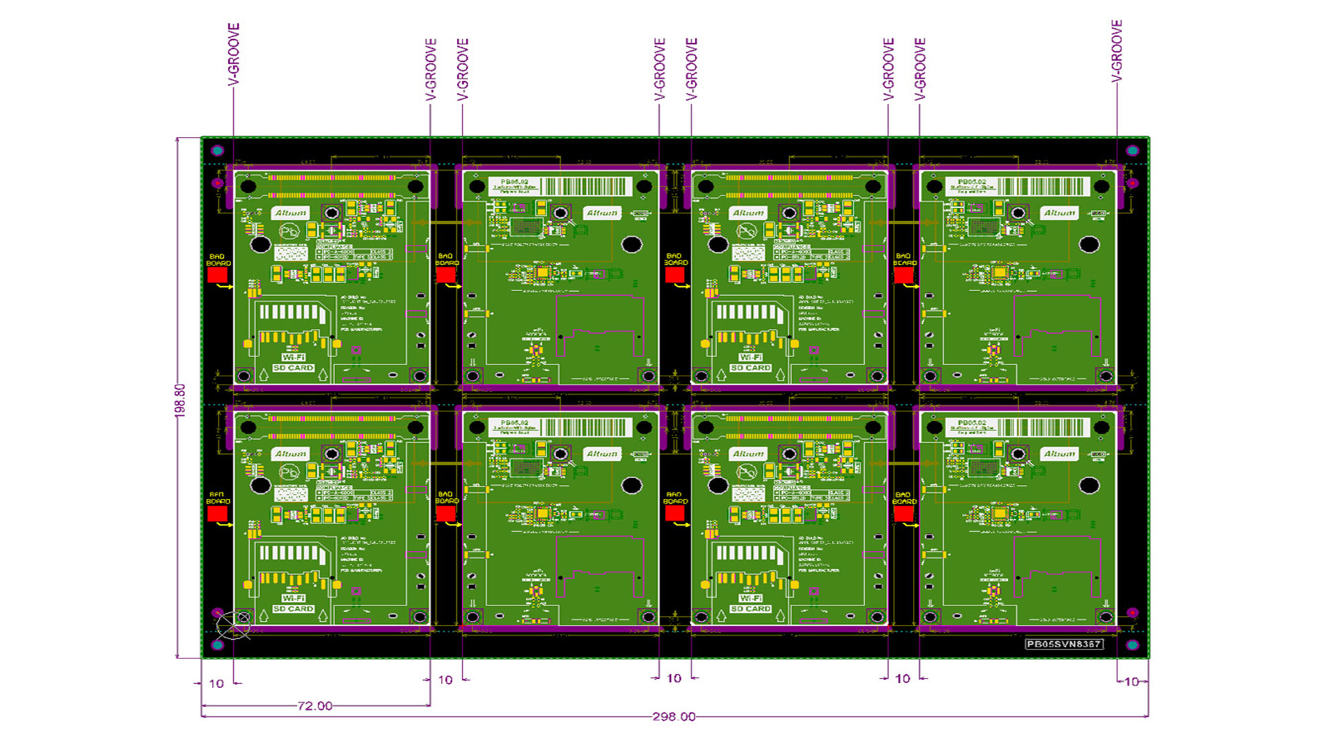
DFM principles guide the arrangement of boards on a panel to ensure maximum output with minimal waste. This includes proper spacing between boards (typically 2-3 mm for V-cut separation or 5-10 mm for routed edges) to prevent damage during depanelization. It also involves aligning designs to avoid weak spots or stress points that could lead to cracks during handling.
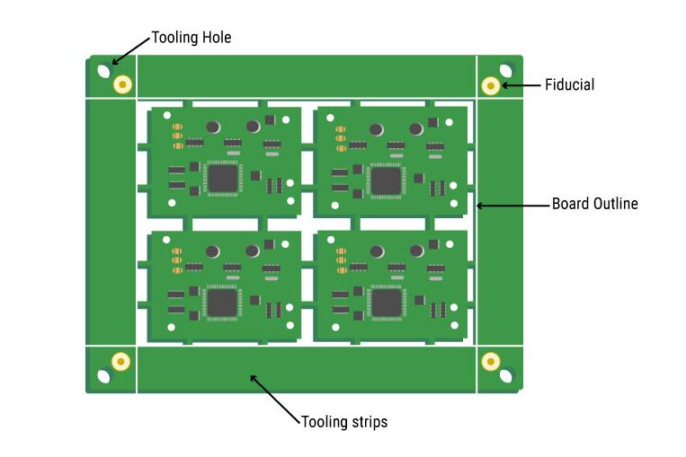
For instance, DFM might dictate the inclusion of tooling holes or fiducial marks on the panel for precise alignment during assembly. These small design tweaks can reduce machine setup errors by up to 30%, ensuring smoother production runs and fewer delays.
2. Reducing Manufacturing Errors
A well-executed DFM strategy anticipates potential manufacturing challenges and addresses them at the design stage. For panelized boards, this could mean ensuring uniform copper distribution across the panel to prevent warping during reflow soldering. Warping can cause components to misalign, leading to failure rates as high as 10-15% in poorly balanced designs.
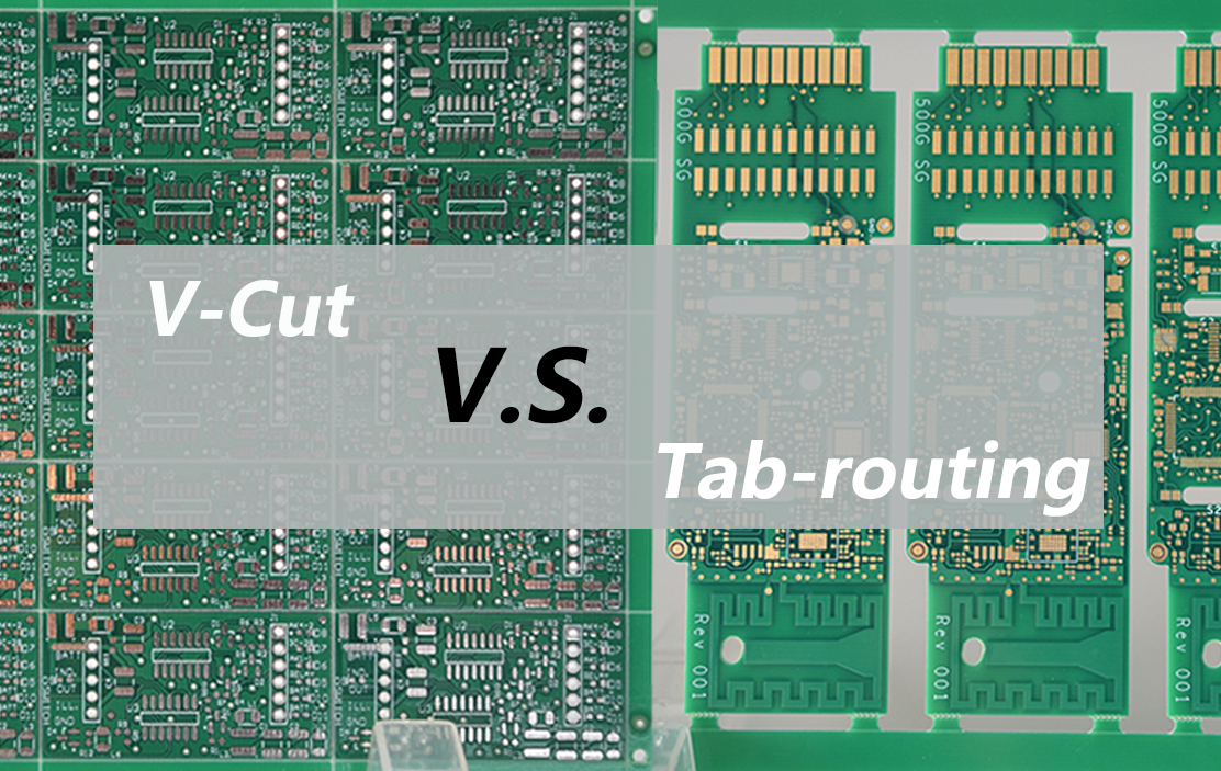
DFM also considers the depanelization method—whether V-cut, tab-routing, or breakaway tabs—and designs the panel to minimize stress on components near the edges. By reducing errors upfront, DFM saves time and resources that would otherwise be spent on troubleshooting or scrap.
3. Accelerating Time-to-Market
Speed is critical in electronics, where product lifecycles are often short. DFM streamlines the transition from design to production by ensuring that panelized boards are ready for manufacturing without extensive revisions. For example, adhering to standard panel sizes and design rules can cut pre-production lead times by 1-2 days, allowing prototypes or final products to reach the market faster.
When DFM and panelization work hand in hand, the entire manufacturing process—from fabrication to assembly—becomes a seamless operation. This synergy is especially valuable for industries like consumer electronics, where rapid iteration and delivery are essential.
Practical Tips for Effective Panelization and DFM
To fully harness the benefits of panelization and DFM, careful planning and execution are necessary. Here are some actionable tips to ensure your PCB projects achieve optimal cost cutting, material utilization, and manufacturing efficiency.
- Collaborate Early with Manufacturers: Share your design files and discuss panelization requirements before finalizing layouts. Manufacturers can provide insights on panel sizes, separation methods, and material constraints to avoid costly redesigns.
- Use Standard Panel Sizes: Stick to common panel dimensions (e.g., 18 x 24 inches) to maximize material utilization and avoid custom tooling costs, which can add 10-20% to production expenses.
- Incorporate DFM Checklists: Use software tools or manual checklists to verify spacing, edge clearance, and component placement. This can reduce manufacturing defects by up to 25%.
- Plan for Depanelization: Choose the right separation method based on board size and component proximity. V-cut is ideal for straight edges, while tab-routing suits irregular shapes, minimizing stress on delicate components.
- Test Panel Designs: For high-volume runs, produce a small batch of panels to identify potential issues like misalignment or thermal stress before full-scale production.
Challenges to Watch Out For in Panelization
While panelization offers numerous benefits, it’s not without challenges. Being aware of these potential pitfalls can help you mitigate risks and maintain efficiency.
First, improper panel design can lead to stress during depanelization, damaging components or traces near board edges. For example, placing sensitive parts too close to a V-cut line can result in microcracks, increasing failure rates by 5-10%. DFM can address this by enforcing minimum clearance rules.
Second, over-optimizing a panel for material utilization can sometimes backfire. Crowding too many boards onto a panel may leave insufficient space for tooling or handling, slowing down automated processes and increasing error rates. A balanced approach, guided by DFM, is essential.
Finally, not all designs are suitable for panelization. Very large or uniquely shaped boards may require custom panels, driving up costs. In such cases, weigh the benefits of panelization against the expense of tailored solutions.
Conclusion: Maximizing Speed and Efficiency with Panelization and DFM
Panelization is a game-changer in PCB manufacturing, delivering undeniable benefits in cost cutting, material utilization, and manufacturing efficiency. By grouping multiple boards onto a single panel, manufacturers can streamline production, reduce waste, and accelerate timelines—often cutting assembly times by half and boosting board yield by 20%. When paired with Design for Manufacturability, these advantages are amplified through optimized layouts, fewer errors, and faster time-to-market.
For engineers and businesses looking to stay competitive, adopting panelization and DFM isn’t just a smart choice—it’s a necessity. By focusing on efficient design practices and collaborating closely with manufacturing partners, you can unlock significant savings and ensure high-quality results for every project. Whether you’re working on prototypes or high-volume production, these strategies will help you achieve your goals with speed and precision.