ALLPCB


Buying a health watch and monitoring physiological parameters does not by itself make you healthier. The key is to monitor certain physiological metrics over extended periods, learn their typical ranges, and use that information to adjust daily habits to improve outcomes. This process helps to understand how the body operates and how to reduce long-term health costs.
Overview of ADI wearable VSM platform
This article describes ADI's latest wearable VSM platform and associated sensor technologies. The platform is intended as a reference to help electronics designers and system architects accelerate development of more accurate and intelligent wearable devices for professional and medical markets.
What to measure, how, and where
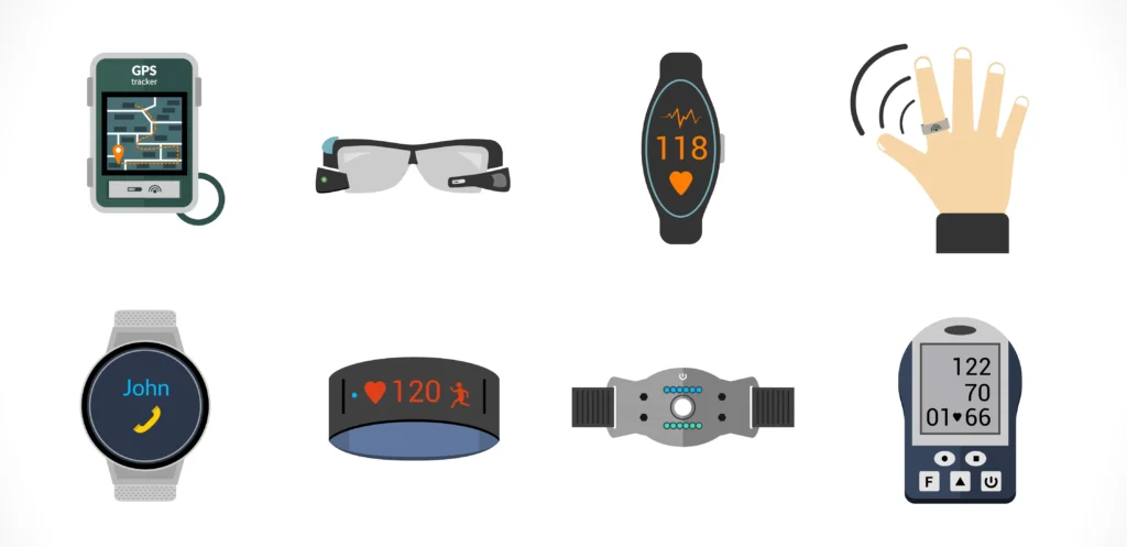
Wearable devices can measure a variety of important physiological parameters. Depending on the overall goal, some parameters are more important than others. The placement of the device on the body largely determines which parameters can be measured.
The wrist is the most obvious location. Wrist-worn devices are familiar to users, so many products are available as smartwatches and wristbands.
The head is another suitable location. Headphones and earbuds often contain embedded sensors to measure heart rate, oxygen saturation, temperature, and related parameters.
The chest is a third suitable location. First-generation heart rate monitors were chest straps; this bioelectric measurement method remains highly accurate. Chest patches are now more common because straps can be uncomfortable. Several manufacturers offer smart chest patches for monitoring key physiological parameters.
Body location influences not only which parameters can be measured but also which measurement technologies are appropriate.
Bioelectric versus optical for heart rate
For heart rate, bioelectric measurements are among the oldest techniques. The signal is strong and can be captured using two or more electrodes. This approach is best implemented in a chest strap or in-ear device, but it is nearly impossible to obtain reliable bioelectric signals from a single point on the wrist because electrodes must be placed near the heart to detect the electrical activity.
For single-point measurements, optical methods are more suitable. Light is transmitted into tissue and the reflected signal from arterial blood flow is measured. From the received optical signal, beat-by-beat heart rate information can be derived. Although this technique seems straightforward, it is challenged by motion artifacts and ambient light, which complicate the design.
ADI's second-generation wearable reference platform integrates most of these technologies. The device is designed for wrist wear, but the band can be removed and the device used as a chest patch. The platform supports bioelectric measurement, optical heart rate, bioimpedance, motion tracking, and temperature sensing, all integrated into a battery-powered miniature device.
Purpose of the platform
The platform is designed to evaluate different sensing techniques and to enable simultaneous measurement of multiple key parameters. Measurements can be stored in flash or transmitted via BLE to a smart device. Concurrent measurements also help identify correlations between parameters. Biomedical engineers, algorithm providers, and companies seek new technologies and use cases to detect disease earlier and reduce adverse effects. The sensor suite of the second-generation wearable supports these efforts.
Sensor stack and board design
The second-generation wearable is built around two stacked printed circuit boards. The main board contains a low-power processor, BLE wireless, and a complete power management subsystem, including battery conditioning and charging. The sensor board supports all measurement technologies.
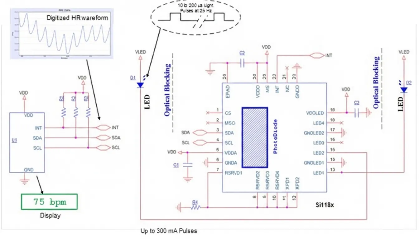
Optical PPG system
The PPG optical system centers on ADI's second-generation analog front end, the ADPD107. The ADPD series functional block diagram is shown below.
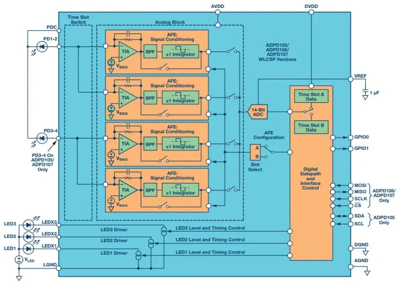
Figure 1. ADPD105/ADPD106/ADPD107 functional block diagram
The ADPD107 acts as a complete transceiver, driving LEDs and measuring the returned photocurrent from photodiodes. The goal is to measure as much photogenerated current as possible for a given LED drive current. The input receive chain uses a configurable transimpedance amplifier with four programmable gain steps up to 200k. The second stage suppresses ambient light. Ambient light interference is a major problem, especially when illumination is modulated. The ambient suppression module includes a band-pass filter followed by an integrator to support synchronous demodulation. This function effectively suppresses external light interference and can be fully bypassed when not required.
The optical system uses light pulses. It provides three programmable LED current sources with programmable maximum currents up to 370 mA and pulse widths down to 1 μs. For good signal response, pulse widths of about 2 μs to 3 μs are recommended. A sequence of LED pulses is typically issued while an ADC samples the photodiode receive signals associated with those pulses. A digital engine averages multiple samples to improve effective resolution.
Mechanical design also significantly affects optical performance. The second-generation device uses discrete optical components, providing flexibility in photodiode selection and LED wavelengths and relaxing mechanical constraints such as spacing between LEDs and photodiodes. The platform supports two green LEDs, one red LED, and one infrared LED. For designers with limited optical design experience, an integrated optical module may be easier to use.
Choices for photodiode count, size, and LED wavelengths were driven by the need to maintain good optical performance even when mounted behind a plastic window. First-generation designs required a separate inner window to suppress internal light contamination, which helped reduce DC offset from light that did not penetrate tissue. Separate windows are difficult and costly to integrate. Newer modules (for example ADPD144RIZ and ADPD175GIZ) have improved to operate with a single full window and minimal internal light path (ILP) effects.
Bioelectric front end for ECG
Two AD8233 analog front ends support bioelectric measurements. The AD8233 is ADI's second-generation single-lead ECG front end with an integrated right-leg drive (RLD), designed to extract, amplify, and filter weak bioelectric signals in high-noise environments. Target applications include wearables, portable home care systems, and training equipment. The AD8233 operates in AC-coupled configurations. The input stage has two gain stages: the first stage has limited gain followed by a second-order high-pass filter and a second gain stage. The input module provides an overall gain of 100 V/V while removing offset from electrode half-cell potentials. The second stage includes a third-order low-pass filter realized as a second-order Sallen-Key filter plus an additional low-pass element to suppress EMG-related signals from muscle activity.
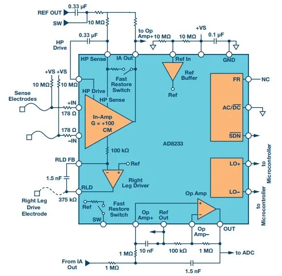
Figure 2. AD8233 ECG front-end functional block diagram
The operating frequency band of the bioelectric front end depends on the use case. A basic heart rate monitor that only needs QRS detection operates over a much smaller bandwidth than an ECG monitor that requires timing and amplitude information from P waves, QRS complexes, and T waves. The AD8233 bandwidth is set by external resistors and capacitors. For flexibility, the wearable platform configures one AD8233 with embedded electrodes for a motion bandwidth supporting 7 Hz to 25 Hz. The second AD8233 can be used with external electrodes to monitor 0.5 Hz to 40 Hz signals. In principle, nearly any bandwidth can be selected by modifying the R and C values on the hardware.
Depending on precision requirements, the AD8233 output can be routed to the sensor board's Cortex-M3 processor embedded 12-bit SAR ADC, or digitized by a standalone 16-bit AD7689 SAR ADC. Users can trade off precision versus battery life.
The device includes two electrodes on the back with dual purposes: in addition to ECG, they can measure electrodermal activity (EDA).
EDA and skin conductance
Electrodermal activity, also called galvanic skin response, relates to skin conductance. Emotional changes caused by internal or external stimuli temporarily change skin conductance; for example, stress or seizures alter skin impedance. The second-generation device can detect these small conductance changes. The system applies an AC excitation to two dry electrodes. Wet electrodes yield better results, but the platform uses two embedded stainless steel dry electrodes. The key advantage of AC excitation is that it prevents electrode polarization. The receive chain is a transimpedance amplifier followed by an AD7689 16-bit SAR ADC. For performance, the ADC sampling rate is much higher than the excitation frequency. The ADC output feeds a discrete Fourier transform (DFT) engine running on an ADuCM3029 processor to represent complex impedance. This method measures skin impedance or conductance with high signal-to-noise ratio while effectively rejecting 50 Hz/60 Hz ambient interference.
The circuit for this measurement is implemented with discrete components to provide flexibility, precision, and low power consumption. ADI is also developing a new chip to support these applications with high precision and very low power. The ADuCM350 supports similar measurements but is not optimized for power-sensitive applications.
Motion sensing
Measuring vital signs without knowing the activity state of the body limits the value of wearable data. Motion detection and analysis are therefore important. Optical heart-rate scenarios are highly sensitive to motion, which can completely corrupt measurements. Motion must be tracked to compensate artifacts. Motion sensors help track activity and can be used to compensate final readings when required.
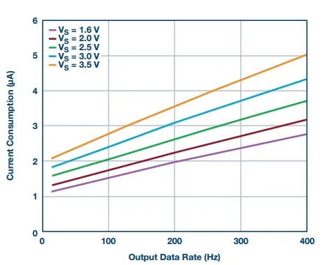
The ADXL362 is an ultra-low-power motion sensor with a 3-axis MEMS accelerometer and an integrated 12-bit ADC to detect X, Y, and Z motion. ADC output data rate (ODR) reflects power consumption; at full ODR of 400 Hz per axis, power consumption is 3 μA. The sensor can also act as a motion wake-up switch. Sampling rates can be reduced to 6 Hz. Every 150 ms the sensor wakes, measures motion, and returns to sleep if no motion is detected. If acceleration exceeds a threshold for a minimum duration, the sensor generates an interrupt or enables a power switch to wake the application. In this mode, the sensor consumes only 300 nA, enabling years of operation on a single coin cell battery. Considering these use cases, motion sensors are essential in wearables.
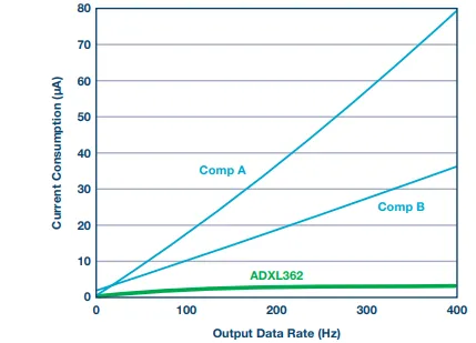
Figure 3. ADXL362 power versus output data rate
Temperature sensing
Temperature is another important parameter. The second-generation wearable includes two temperature sensors. The wrist device uses NTC thermistors to measure skin temperature and internal device temperature. There are multiple methods to measure temperature via skin contact. NTCs are powered and conditioned with discrete circuits, and a 16-bit ADC digitizes the signal. ADI offers a range of temperature sensor types and accuracy levels. Temperature sensors in the second-generation platform are discrete to enable reuse of ADCs and other functions, reducing redundancy and saving power.
ADuCM3029 processor
The second-generation device uses two processors to provide flexibility. The BLE interface board contains a processor, and the sensor board contains a processor to enable autonomous operation.
The platform integrates a very low-power ADuCM3029 to collect sensor data and run algorithms. The processor integrates multiple modules as summarized below.
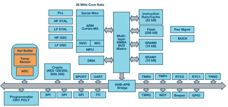
Figure 4. ADuCM3029 integrated modules
The core is a 26 MHz Cortex-M3 with a rich set of peripherals, on-chip memory, and analog front end. It supports four operating modes. In full operation mode, the chip consumes 38 μA/MHz. If processing is not required, the platform can run in a flexible mode where the analog front end and peripherals remain active and measured signals are stored in memory via DMA. This mode consumes only 300 μA, making the chip attractive for low-power battery systems. The processor also includes multiple security features to protect code and a hardware accelerator for cryptographic functions.
Use case selection
The second-generation wearable supports many use cases. Sensors can be integrated into smartwatches, and functionalities such as precise heart rate monitoring and activity/calorie tracking are useful for sports watches. The main distinction between smartwatches and sport watches is the tradeoff between accuracy and battery life.
Stress or emotional state measurement typically combines multiple signals, for example skin conductance, heart rate variability, and temperature, to obtain reliable readings.
Blood pressure monitoring is an important parameter but is difficult to integrate into continuous wearable systems when based on wrist devices. Some techniques do not require a cuff and can measure blood pressure using pulse transit time (PTT), which requires both ECG and PPG measurements. The sensors on the second-generation platform support this technique.
Applications for elder care and independent living are in demand. Systems that help caregivers remotely monitor certain parameters are valuable. The wearable supports approximately 95% of required functionality for these applications. The system can monitor multiple vital signs, detect whether a person is moving or walking, and detect falls. One missing feature in the reference wearable is an emergency button, which can be implemented by connecting a processor I/O pin to a switch on the device enclosure.
From prototype to product
The second-generation wearable integrates many high-performance sensors and features into a small system. Mechanical design considerations were addressed in addition to electronics. This makes the platform useful for companies designing devices for semi-professional sports, medical markets, smart buildings, independent living, and elder care. All parameters can be measured simultaneously, but algorithms are needed to support specific use cases. Developers and device manufacturers can use this platform to start projects and test and validate algorithms before committing to custom hardware.