ALLPCB


What Is a Phase Change?
A phase change is the process by which a material transforms from one physical state to another as external parameters such as temperature, pressure, or magnetic field vary. Common examples are the transitions among gas, liquid, and solid. In certain materials, these phase changes are accompanied by changes in electrical and optical properties, and those changes are the basis for phase-change memory technologies.
Phase-Change Memory Overview
Phase-change memory (PCM) is a non-volatile memory technology that uses heat generated by electrical pulses to switch a phase-change material between a crystalline (low-resistance) state and an amorphous (high-resistance) state. Data are stored by representing the two states as logical "0" and "1" and are read out by measuring resistance.
The first observations of reversible electrical resistance changes during phase transitions were reported by Stanford Ovshinsky in the late 1960s. Different phase-change materials are used in PCM devices; for example, some implementations use chalcogenide alloys. A common family of materials is germanium-antimony-tellurium, generally referred to as GST. Regardless of composition, PCM relies on the contrast in electrical conductivity between the crystalline and amorphous phases.
In the amorphous state, GST exhibits short-range atomic order and low free-electron density, resulting in high resistivity. This is typically produced by a RESET operation: the device is heated above the melting point and then rapidly quenched to freeze the amorphous phase. Amorphous layer resistance can exceed 1 MΩ. In the crystalline state, GST shows longer-range order and higher free-electron density, producing lower resistivity. SET operations heat the material above the crystallization temperature but below the melting point, then allow it to cool slowly so grains form. Crystalline-state resistance typically ranges from 1 kΩ to 10 kΩ.
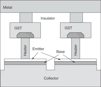
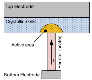
A typical PCM device stack consists of a top electrode, crystalline GST, an active amorphous/crystalline region, a thermal insulator, a resistive heater, and a bottom electrode.
Electrical Characterization of PCM Materials and Devices
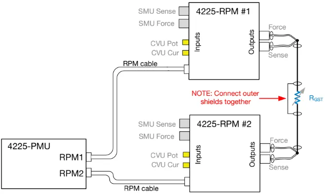
Before normal operation, PCM devices usually require a forming step. Forming creates an active region where the reversible transitions between amorphous and crystalline phases occur. The semicircular shape in the schematic represents this active region. A typical test connection diagram is shown below.
One of the main testing challenges is finding appropriate RESET and SET pulse parameters (amplitude, rise/fall times, pulse width). This is typically an iterative process. The RESET voltage is the largest and must be located carefully. One common method is to apply pulses while gradually increasing amplitude, measuring resistance after each pulse, and stopping once the resistance reaches the desired value. Then reapply pulses to locate the SET conditions.
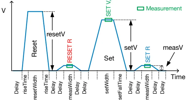
PCM devices are sensitive to pulse width and rise/fall times, so pulse parameters must be set to match the device under test. A typical PCM programming waveform is shown below.
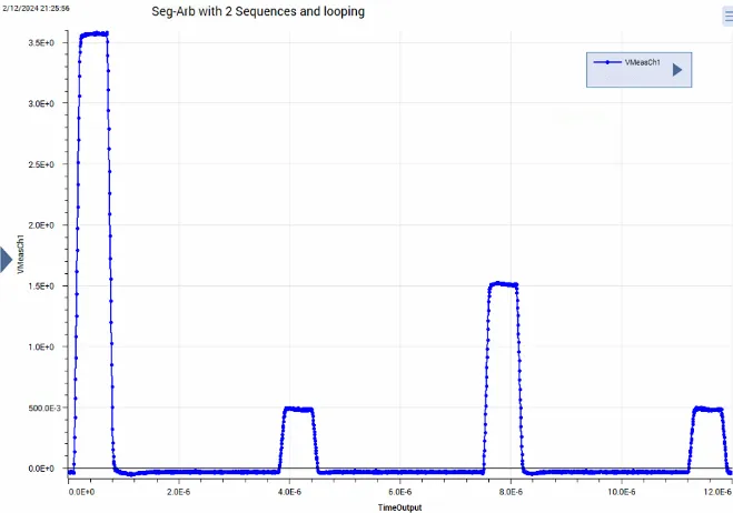
Pulse sequences can be generated with a PMU capable of arbitrary pulse generation. An example pulse-sequence output from a 4200A PMU is shown here.
Typical Test Setup
- 4200A-SCS mainframe with Clarius software
- Two SMUs plus two 4200-PA preamplifiers
- One PMU plus two RPM modules
Advantages of This Configuration
- Low-current measurement capability down to 10 fA
- Clarius software includes a phase-change test project module
- Configuration is commonly used in semiconductor materials and device testing
- Built-in PCM test modules enable fast electrical parameter characterization