ALLPCB


PCB lamination is a critical step in the manufacturing of multi-layer printed circuit boards (PCBs). It involves bonding multiple layers of material together under heat and pressure to create a single, cohesive board. However, this process is prone to various issues that can compromise the quality and functionality of the final product. So, what can go wrong with PCB lamination? Common problems include delamination, voids, warpage, line width issues, surface preparation challenges, and defects in the DES (Develop, Etch, Strip) process. In this comprehensive guide, we’ll dive deep into these potential pitfalls, explain their causes, and offer practical solutions to ensure high-quality multi-layer boards.
Understanding PCB Lamination in Multi-Layer Boards
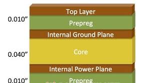
Before exploring the issues, let’s briefly understand the PCB lamination process, especially for multi-layer boards. A multi-layer PCB consists of multiple layers of conductive copper and insulating materials (like prepreg and core laminates) stacked and bonded together. The lamination process uses heat (typically 180-200°C) and pressure (around 300-500 psi) to fuse these layers into a solid structure. This step is vital for ensuring electrical connectivity and mechanical stability.
However, even small errors in this process can lead to significant defects. For engineers and manufacturers, recognizing these potential issues early can save time, reduce costs, and improve reliability. Let’s break down the most common problems associated with PCB lamination.
Common Defects in PCB Lamination
1. Delamination: When Layers Fail to Bond
Delamination is one of the most severe issues in PCB lamination. It occurs when layers of the board separate, either between the substrate layers or between the copper foil and the substrate. This defect can lead to electrical failures, reduced mechanical strength, and even complete board failure.
Causes of Delamination:
- Improper Surface Preparation: If the copper foil or substrate surface isn’t clean or roughened properly before lamination, bonding can be weak. For instance, oil, dust, or oxidation on the surface can prevent strong adhesion.
- Moisture Contamination: Moisture trapped in the materials (especially prepreg) can vaporize during the high-temperature lamination process, creating bubbles or separation.
- Inadequate Heat or Pressure: If the lamination press doesn’t reach the required temperature or pressure, the layers may not bond fully.
Solutions:
- Ensure thorough cleaning and roughening (micro-etching) of copper surfaces to improve adhesion.
- Store materials in a controlled environment to minimize moisture absorption, and consider pre-baking prepreg at 120°C for 2-4 hours before lamination.
- Calibrate lamination equipment to maintain consistent heat and pressure settings within manufacturer-recommended ranges.
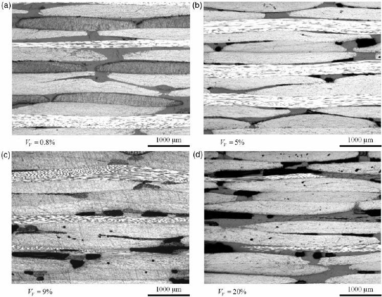
2. Voids and Air Bubbles: Trapped Imperfections
Voids are empty spaces or air bubbles trapped between layers during lamination. These defects can weaken the board’s structure and disrupt electrical performance by creating areas of inconsistent dielectric properties.
Causes of Voids:
- Incomplete Resin Flow: If the resin in the prepreg doesn’t flow evenly during lamination, air can get trapped.
- Insufficient Vacuum: Many lamination processes use a vacuum to remove air, but if the vacuum is inadequate, bubbles remain.
- Material Defects: Poor-quality prepreg or core materials may have uneven resin distribution, leading to voids.
Solutions:
- Use high-quality materials with consistent resin content (typically 40-50% by weight for prepreg).
- Optimize vacuum settings during lamination to ensure air removal, often maintaining a vacuum level of 25-28 inches of mercury (inHg).
- Adjust lamination temperature and pressure profiles to allow proper resin flow without rushing the process.
3. Warpage: Distortion of the Board
Warpage occurs when the PCB becomes uneven or distorted after lamination, making it difficult to assemble components or mount the board in a device. This defect often results from uneven stress distribution during the lamination process.
Causes of Warpage:
- Asymmetrical Layer Stackup: If the layer stack isn’t balanced (e.g., different copper densities on opposite sides), thermal expansion can cause bending.
- Uneven Cooling: Rapid or uneven cooling after lamination can create internal stresses.
- Inconsistent Material Properties: Using materials with mismatched coefficients of thermal expansion (CTE) can lead to distortion. For example, a CTE mismatch of more than 10 ppm/°C between layers can cause significant warpage.
Solutions:
- Design a balanced stackup with symmetrical copper distribution (e.g., similar copper thickness on top and bottom layers).
- Implement controlled cooling rates (e.g., 2-3°C per minute) to minimize thermal stress.
- Select materials with compatible CTE values, ideally within 5 ppm/°C of each other.
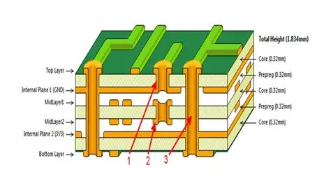
Specific Challenges in Registered Multi-Layer Boards
Multi-layer boards require precise registration, meaning all layers must align perfectly to ensure vias and traces connect as intended. Misalignment during lamination can lead to functional failures, especially in high-density designs.
Causes of Misalignment:
- Inaccurate Positioning Pins: If the pins used to hold layers in place are too short or loose, layers can shift during lamination.
- Tooling Hole Issues: Deformed or improperly placed tooling holes can cause misalignment.
- Thermal Expansion: Layers may expand at different rates during heating, leading to misalignment if not accounted for in the design.
Solutions:
- Use longer, high-precision positioning pins and regularly inspect them for wear.
- Verify tooling hole accuracy with automated optical inspection (AOI) systems before lamination.
- Account for thermal expansion in the design phase by adding appropriate scaling factors (typically 0.02-0.05% per layer).
Line Width Issues During Lamination
Line width issues refer to deviations in the width of copper traces on the PCB, which can affect signal integrity and impedance. While lamination itself doesn’t directly cause line width problems, the heat and pressure involved can exacerbate pre-existing issues from earlier manufacturing steps.
Causes of Line Width Issues:
- Over-Etching or Under-Etching: Before lamination, if the etching process isn’t controlled, trace widths may vary beyond acceptable tolerances (e.g., ±10% of design width).
- Pressure-Induced Deformation: Excessive pressure during lamination can compress traces, especially in thinner inner layers, altering their dimensions.
- Material Shrinkage: Some laminates shrink slightly during the process, potentially distorting trace geometries.
Solutions:
- Monitor etching processes closely to maintain line width within ±5% of the target value (e.g., for a 5-mil trace, keep variation below 0.25 mil).
- Optimize lamination pressure to avoid over-compression, typically staying below 400 psi for sensitive designs.
- Use low-shrinkage materials (e.g., high-Tg FR-4 with shrinkage rates below 0.1%) to minimize dimensional changes.
Issues with Surface Preparation Before Lamination
Surface preparation is a crucial step before lamination, as it directly impacts how well the layers bond. Poor preparation can lead to many of the defects already discussed, like delamination and voids.
Common Surface Preparation Issues:
- Contamination: Oil, dust, or fingerprints on copper or substrate surfaces can weaken adhesion.
- Inadequate Roughening: If the copper surface isn’t properly roughened (via micro-etching or black oxide treatment), the resin may not grip effectively.
- Oxidation: Exposed copper can oxidize if not treated promptly, reducing bond strength.
Solutions:
- Implement strict cleaning protocols using solvents or plasma cleaning to remove contaminants.
- Use micro-etching to achieve a surface roughness of 1-2 μm for optimal resin adhesion.
- Apply anti-oxidation coatings or store cleaned layers in a controlled environment to prevent oxidation.
DES Process Defects and Their Impact on Lamination
The DES (Develop, Etch, Strip) process is used to pattern copper layers before lamination. Defects in this process can create issues that become evident during or after lamination, affecting the board’s performance.
Common DES Process Defects:
- Under-Development: If the photoresist isn’t fully developed, unwanted copper may remain, leading to shorts or incorrect trace patterns.
- Over-Etching: Excessive etching can thin traces or create breaks, impacting signal integrity (e.g., increasing impedance beyond the target 50 ohms for high-speed signals).
- Resist Residue: Leftover photoresist after stripping can interfere with surface bonding during lamination.
Solutions:
- Optimize development time and chemical concentration to ensure complete photoresist removal without overexposure.
- Control etching parameters (e.g., etchant temperature at 50-55°C and spray pressure at 2-3 bar) to avoid over-etching.
- Use thorough stripping and cleaning processes to remove all resist residue before lamination.
How to Prevent PCB Lamination Issues
Preventing lamination defects requires a combination of good design practices, high-quality materials, and precise manufacturing controls. Here are some overarching tips to minimize risks:
- Design for Manufacturability (DFM): Follow DFM guidelines to ensure your layer stackup, trace widths, and material choices are compatible with lamination processes.
- Material Selection: Choose laminates and prepregs with consistent properties, such as a dielectric constant (Dk) of 4.2-4.5 for standard FR-4 materials, to ensure predictable performance.
- Process Monitoring: Use real-time monitoring tools during lamination to track temperature, pressure, and vacuum levels, ensuring they stay within specified ranges (e.g., ±5°C for temperature).
- Quality Checks: Perform post-lamination inspections, such as X-ray or microsection analysis, to detect hidden defects like voids or delamination early.
Conclusion
PCB lamination is a complex but essential part of manufacturing multi-layer boards. While many things can go wrong—ranging from delamination and voids to line width issues, surface preparation challenges, and DES process defects—most of these problems are preventable with careful planning and execution. By understanding the causes of these issues and implementing the solutions outlined in this guide, engineers and manufacturers can achieve higher yields and more reliable PCBs. Whether you’re dealing with warpage in a registered multi-layer board or surface prep issues, the key lies in attention to detail at every step of the process.
With the right approach, you can minimize the risks associated with PCB lamination and ensure your boards meet the highest standards of quality and performance. Trust in proven practices and advanced manufacturing techniques to tackle these challenges head-on.