 ALLPCB


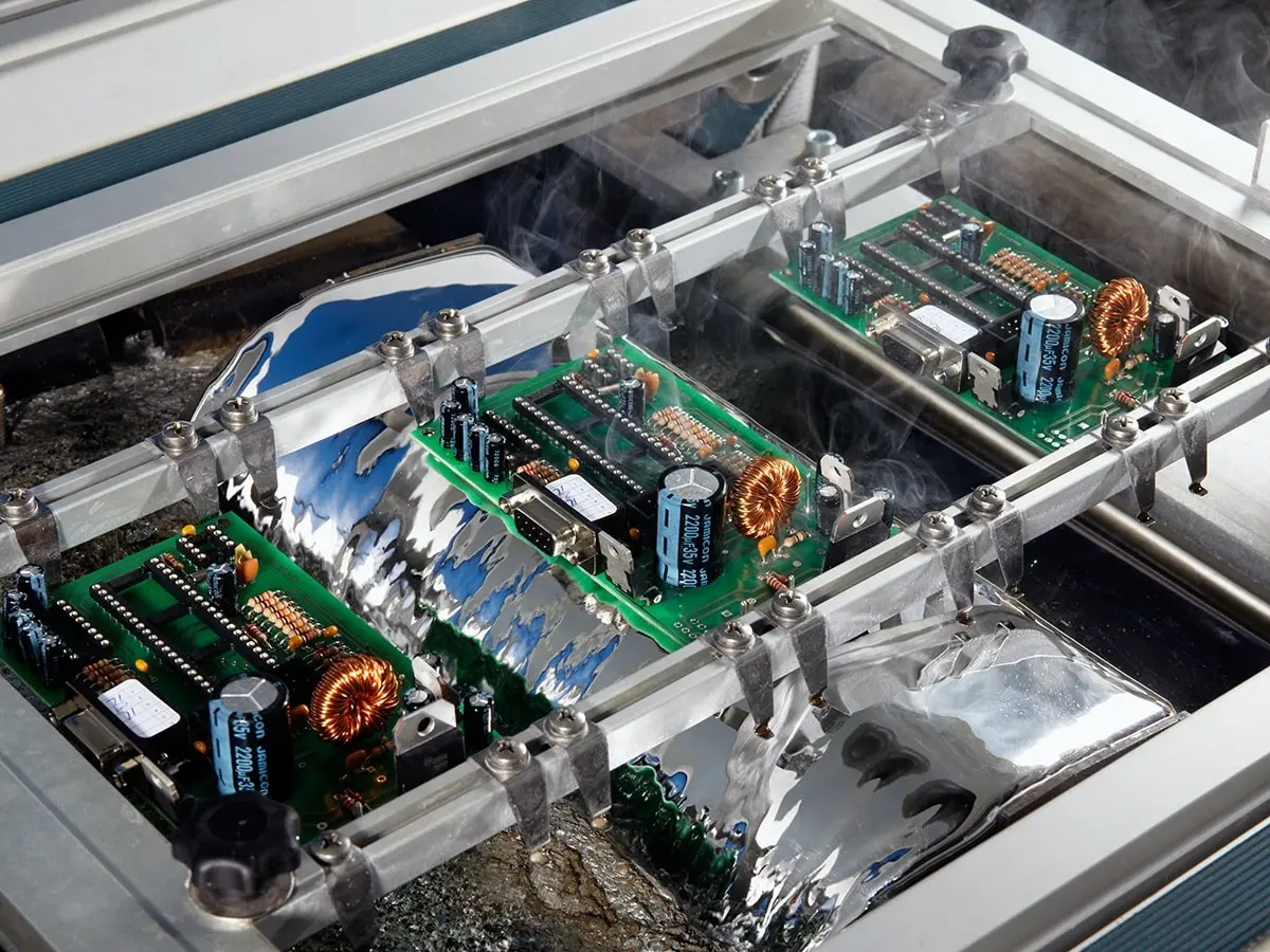
Wave soldering is a vital process in electronics manufacturing, especially for assembling through-hole components on printed circuit boards (PCBs). However, defects during wave soldering can lead to costly rework, delays, and reduced product reliability. If you're searching for a wave soldering defects guide or solutions to issues like wave soldering temperature defects, flux wave soldering defects, or solder mask defects, you've come to the right place. This comprehensive blog will help you identify common wave soldering problems, troubleshoot their causes, and optimize process parameters for flawless results. Let's dive into the details of preventing wave solder defects and ensuring high-quality PCB assembly.
What Is Wave Soldering and Why Do Defects Happen?
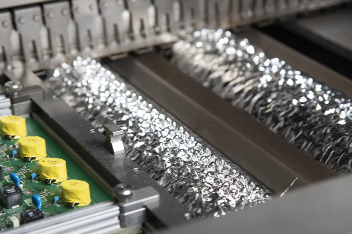
Wave soldering is an automated soldering method used in high-volume PCB assembly. It involves passing a PCB over a molten solder wave to create reliable joints between through-hole components and the board. The process includes several stages: flux application to clean surfaces, preheating to avoid thermal shock, soldering with the molten wave, and cooling to solidify the joints.
Despite its efficiency, wave soldering is prone to defects. Studies suggest that up to 50% of PCB assembly defects can originate from this process due to factors like improper temperature settings, poor flux application, or design flaws. Understanding these issues is the first step to troubleshooting and optimizing your manufacturing process.
Common Wave Soldering Defects and Their Causes
Let's explore the most frequent wave soldering defects, their root causes, and how they impact PCB quality. This section serves as a detailed wave soldering defects guide for engineers looking to improve their assembly process.
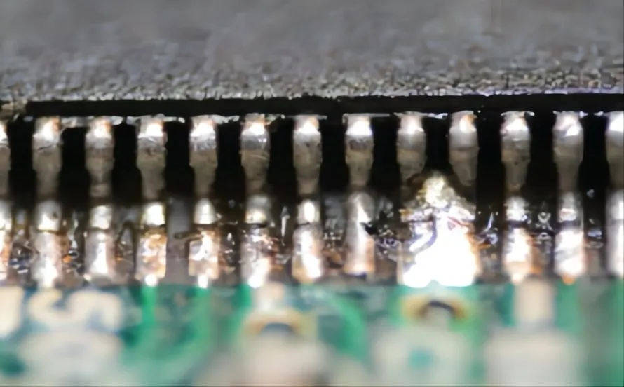
1. Solder Bridging
Solder bridging occurs when excess solder creates unintended connections between adjacent pins or pads, leading to short circuits. This is one of the most common issues in wave soldering.
- Causes: Too high solder wave height, incorrect PCB orientation, or closely spaced components.
- Impact: Short circuits can cause complete device failure.
2. Insufficient Solder or Cold Joints
Insufficient solder results in weak or incomplete joints, often due to wave soldering temperature defects. Cold joints appear dull and grainy, indicating poor bonding.
- Causes: Low solder temperature (ideal range is typically 250-260°C), inadequate preheating, or contaminated surfaces.
- Impact: Weak joints may fail under stress, leading to intermittent connections.
3. Solder Skips
Solder skips happen when certain areas of the PCB fail to receive solder, leaving pins or pads unconnected.
- Causes: Shadowing effects from taller components, poor flux application, or low wave height.
- Impact: Unconnected components result in non-functional circuits.
4. Excess Solder or Icicles
Excess solder can form lumps or icicles on component leads, increasing the risk of shorts and adding unnecessary weight to the PCB.
- Causes: High solder wave height, slow conveyor speed, or improper cooling.
- Impact: Adds cost due to material waste and potential rework.
5. Flux-Related Defects
Flux wave soldering defects are common when flux is not applied correctly or is of poor quality. Flux cleans surfaces for better solder adhesion, but issues can lead to defects.
- Causes: Insufficient flux, expired or low-quality flux, or uneven application.
- Impact: Poor wetting results in weak joints or solder skips.
Troubleshooting Wave Soldering Defects: Step-by-Step Solutions
Now that we've identified common defects, let's look at actionable solutions to troubleshoot and prevent them. This section offers practical tips for preventing wave solder defects.
1. Optimize Temperature Settings to Avoid Wave Soldering Temperature Defects
Temperature control is critical in wave soldering. If the solder bath is too cold (below 250°C), it can cause cold joints or insufficient solder. If it's too hot (above 260°C), it risks damaging components or the PCB.
- Solution: Use a thermal profiler to monitor solder bath and preheat temperatures. Maintain solder bath at 250-260°C and preheat to 100-120°C to avoid thermal shock.
- Tip: Regularly calibrate temperature sensors to ensure accuracy.
Related Reading: Optimizing Wave Soldering Temperature: A Key Factor for Reliable PCB Joints
2. Improve Flux Application to Prevent Flux Wave Soldering Defects
Flux prepares the PCB surface for soldering by removing oxides. Poor flux application can lead to uneven soldering or skips.
- Solution: Use a spray or foam fluxer for even coverage. Check flux density (typically 500-1500 micrograms per square inch) and replace old or contaminated flux.
- Tip: Clean flux residues after soldering to prevent corrosion over time.
3. Adjust Conveyor Speed and Wave Height
Conveyor speed and wave height directly affect solder application. Too fast a speed or low wave height can cause skips, while slow speed or high wave height leads to excess solder.
- Solution: Set conveyor speed to 1.0-1.5 meters per minute for most PCBs. Adjust wave height so it contacts the PCB bottom without flooding.
- Tip: Test with a sample board to fine-tune these parameters.
4. Address Solder Mask Defects
Solder mask defects occur when the protective layer on a PCB fails to prevent solder from adhering to unwanted areas, often due to poor mask application or damage during handling.
- Solution: Ensure the solder mask is fully cured before wave soldering. Inspect for pinholes or scratches that could expose copper. Use a mask thickness of 0.8-1.2 mils for optimal protection.
- Tip: Store PCBs in a controlled environment to avoid mask degradation.
Optimizing Process Parameters for Flawless Wave Soldering
Beyond troubleshooting specific defects, optimizing the entire wave soldering process can significantly reduce errors. Here's how to fine-tune key parameters for consistent quality.
1. Fine-Tune Preheating Parameters
Preheating prevents thermal shock, which can crack components or warp the PCB. It also activates flux for better wetting.
- Optimal Range: Preheat to 100-120°C over 60-90 seconds, depending on board thickness (1.6mm boards typically need 60 seconds).
- Benefit: Reduces temperature gradients, minimizing defects like cold joints.
2. Select the Right Solder Alloy
The choice of solder alloy impacts joint reliability and defect rates. Lead-free solders, for instance, require higher temperatures than traditional tin-lead alloys.
- Optimal Choice: Use SAC305 (Sn96.5/Ag3.0/Cu0.5) for lead-free soldering, maintaining a bath temperature of 255-260°C.
- Benefit: Balances cost, reliability, and compliance with environmental regulations.
3. Maintain Equipment Regularly
Wave soldering machines require consistent maintenance to prevent issues like contamination or temperature instability.
- Practice: Clean the solder bath weekly to remove dross (oxide buildup), which can contaminate joints. Check wave nozzles for blockages.
- Benefit: Ensures consistent solder flow and reduces defect rates by up to 20%.
4. Design PCBs with Wave Soldering in Mind
PCB design plays a huge role in preventing wave solder defects. Poor layouts can cause shadowing or uneven solder distribution.
- Practice: Orient components perpendicular to the wave direction to minimize shadowing. Space pins at least 2.54mm apart to avoid bridging.
- Benefit: Reduces solder skips and bridging by improving wave contact.
Preventing Wave Solder Defects: Best Practices for Long-Term Success
While troubleshooting fixes immediate issues, adopting best practices ensures long-term defect prevention. Here are key strategies to maintain high-quality wave soldering.
- Train Operators: Ensure staff are trained on equipment settings and defect identification. A skilled operator can spot issues like improper flux coverage before they escalate.
- Use Quality Materials: Invest in high-quality flux, solder, and PCB materials. Low-grade materials often lead to defects like poor wetting or mask failures.
- Implement Process Monitoring: Use real-time monitoring tools to track temperature, wave height, and conveyor speed. Data logging can help identify trends in defect occurrence.
- Conduct Regular Inspections: Inspect soldered boards using automated optical inspection (AOI) systems to catch defects early. A defect rate below 1% is achievable with consistent checks.
Related Reading: Troubleshooting Common Wave Soldering Problems: A Practical Guide for Engineers
Conclusion: Mastering Wave Soldering for Reliable PCB Assembly
Wave soldering is a powerful technique for high-volume PCB assembly, but defects like solder bridging, cold joints, and flux wave soldering defects can undermine its benefits. By following this wave soldering defects guide, you can troubleshoot issues such as wave soldering temperature defects and solder mask defects while optimizing process parameters for consistent results. From fine-tuning temperature and flux application to designing PCBs with wave soldering in mind, these strategies offer a clear path to preventing wave solder defects.
Implementing the solutions and best practices outlined here will help you achieve reliable solder joints, reduce rework costs, and improve overall product quality. Whether you're an experienced engineer or new to PCB manufacturing, mastering wave soldering is within reach with the right knowledge and tools.


