ALLPCB


If you're a PCB designer looking to explore the advantages of blue solder mask, you've come to the right place. This guide will dive into the key benefits, design rules, costs, and application techniques of blue solder mask for printed circuit boards (PCBs). Whether you're aiming to improve aesthetics, enhance functionality, or streamline manufacturing, blue solder mask offers unique potential. Let’s unlock its full value with actionable insights tailored for PCB designers and engineers.
What Is Blue Solder Mask and Why Does It Matter?
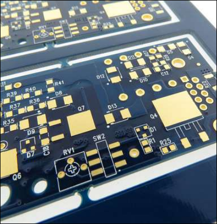
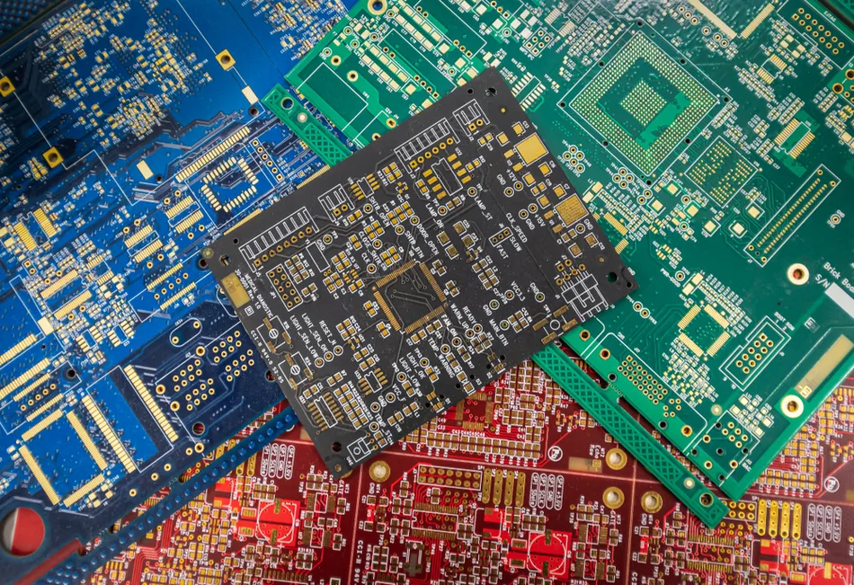
Solder mask is a thin protective layer applied to a PCB to insulate copper traces and prevent solder from bridging between components during assembly. While green has long been the standard color for solder masks, blue solder mask has emerged as a popular alternative. It not only serves the same protective function but also brings distinct advantages in terms of visibility, branding, and design flexibility.
For PCB designers, choosing a blue solder mask can impact both the performance and marketability of the final product. In this comprehensive guide, we’ll cover everything you need to know about blue solder mask benefits, blue solder mask design rules, blue solder mask PCB cost, and blue solder mask application techniques to help you make informed decisions.
The Benefits of Blue Solder Mask for PCB Designers
Opting for a blue solder mask offers several practical and aesthetic advantages. Below, we break down the key blue solder mask benefits that make it a compelling choice for modern PCB designs.
1. Improved Visibility for Inspection
One of the standout benefits of blue solder mask is its high contrast with copper traces and silkscreen markings. This contrast makes it easier to spot defects, misalignments, or soldering issues during visual inspections. For instance, white silkscreen text on a blue background is far more legible than on darker masks like black or green, reducing errors in quality control processes.
2. Aesthetic Appeal and Branding
Blue solder mask provides a sleek, professional look that can align with a company’s branding. Many tech companies choose blue for its modern and clean appearance, which can set their products apart in a competitive market. This is especially relevant for consumer electronics where visual design plays a role in customer perception.
3. Reduced Eye Strain During Assembly
Unlike brighter colors like red or yellow, blue is easier on the eyes under prolonged exposure to factory lighting or during manual assembly. This can improve worker efficiency and reduce fatigue, leading to better overall production quality.
4. Compatibility with Specific Applications
Blue solder mask is often used in industries like automotive and medical devices where distinct color coding is essential for identifying specific board types or functions. This helps in organizing workflows and minimizing mix-ups during manufacturing or maintenance.
Blue Solder Mask Design Rules: Key Guidelines for Success
To fully leverage the benefits of blue solder mask, PCB designers must adhere to specific blue solder mask design rules. These guidelines ensure manufacturability, reliability, and performance. Here are the critical design considerations:
1. Solder Mask Clearance Around Pads
Ensure adequate clearance between solder mask edges and component pads to prevent overlap or misalignment during application. A typical clearance value is 0.1 mm (4 mils) on each side of the pad. This spacing allows for precise soldering and avoids mask residue on pads, which could interfere with solder joint formation.
2. Minimum Feature Size for Openings
The solder mask layer should account for the smallest openings needed for vias or test points. Most manufacturers recommend a minimum opening diameter of 0.3 mm (12 mils) to ensure the mask can be applied accurately without clogging small holes. Check with your fabrication partner for their specific capabilities, as tighter tolerances may increase costs.
3. Avoid Overlapping Silkscreen and Solder Mask
Blue solder mask offers excellent contrast with white silkscreen, but overlapping these layers can cause printing issues. Maintain a clearance of at least 0.15 mm (6 mils) between silkscreen text or symbols and solder mask edges to ensure clarity and prevent smudging during production.
4. Consider Solder Mask Thickness
The thickness of the solder mask layer typically ranges from 0.02 mm to 0.03 mm (0.8 to 1.2 mils). A uniform thickness is crucial for insulation and protection. Designers should specify the desired thickness in their Gerber files and confirm with the manufacturer to avoid variations that could affect signal integrity or component mounting.
5. Account for High-Voltage Applications
For PCBs used in high-voltage environments, ensure the solder mask provides sufficient dielectric strength. Blue solder mask materials are often tested to withstand up to 500V per mil of thickness, but this depends on the specific formulation. Include additional spacing between high-voltage traces (e.g., 0.5 mm or more) to prevent arcing or breakdown.
Understanding Blue Solder Mask PCB Cost: What to Expect
Cost is a critical factor for any PCB project, and the choice of solder mask color can influence the overall budget. Let’s explore the factors that affect blue solder mask PCB cost and how designers can manage expenses without compromising quality.
1. Material and Processing Costs
Blue solder mask is often slightly more expensive than standard green due to the pigments and formulations used. On average, the cost increase can range from 5% to 10% per board, depending on the manufacturer and order volume. However, this cost is often negligible for small to medium batches where the base fabrication cost dominates.
2. Volume and Customization Impact
For large-scale production, the per-unit cost of blue solder mask becomes more competitive as economies of scale come into play. Custom shades of blue or matte finishes may incur additional setup fees, sometimes adding $50 to $100 to the initial tooling cost. Designers should weigh the branding benefits against these incremental expenses.
3. Manufacturer Capabilities
Not all fabricators stock blue solder mask as a standard option, which can lead to longer lead times or higher costs if special orders are required. Partnering with a manufacturer experienced in colored solder masks can help minimize delays and keep costs predictable. Always request a detailed quote that breaks down material and processing fees.
4. Balancing Cost with Quality
While opting for blue solder mask may add a small cost, the benefits of improved inspection and branding often outweigh the expense. Designers can optimize costs by standardizing designs to use common blue shades rather than custom colors, reducing setup fees and material waste.
Blue Solder Mask Application: Techniques and Best Practices
The blue solder mask application process is a critical step in PCB manufacturing that requires precision to achieve consistent results. Understanding the techniques and best practices can help designers prepare files and collaborate effectively with fabricators.
1. Application Methods
Blue solder mask is typically applied using one of two methods: liquid photoimageable (LPI) or dry film. LPI is the most common technique, where the liquid mask is screen-printed or sprayed onto the PCB, then exposed to UV light through a photomask to harden specific areas. This method offers high precision for complex designs with fine features.
Dry film, on the other hand, involves laminating a pre-formed mask layer onto the board, which is then exposed and developed. While less common for colored masks, it can be used for simpler designs or when uniformity is critical.
2. Curing and Hardening
After application, the solder mask undergoes a curing process, typically at temperatures between 120°C and 150°C for 30 to 60 minutes. This step ensures the mask adheres properly to the board and provides the necessary insulation. Designers should confirm that their chosen material can withstand the thermal stresses of curing without cracking or discoloration.
3. File Preparation for Solder Mask Layer
When preparing design files, ensure the solder mask layer is clearly defined in your Gerber or CAD output. Use distinct colors or layer names to differentiate the top and bottom solder mask layers. Include a readme file or fabrication notes specifying the use of blue solder mask to avoid confusion during production.
4. Post-Application Inspection
After the solder mask is applied, manufacturers perform inspections to check for pinholes, uneven coverage, or misalignment. Designers can request detailed inspection reports or specify acceptance criteria, such as a maximum defect size of 0.05 mm, to ensure the blue solder mask meets quality standards.
Challenges and Considerations with Blue Solder Mask
While blue solder mask offers numerous benefits, there are some challenges to keep in mind. Understanding these can help designers mitigate risks and achieve optimal results.
1. Limited Availability
Some manufacturers may not stock blue solder mask as a standard option, leading to longer lead times or higher costs. Early communication with your fabrication partner is essential to confirm availability and plan accordingly.
2. Color Consistency
Different batches of blue solder mask can vary slightly in shade due to differences in pigment or curing conditions. If color consistency is critical for branding, request samples or specify a particular shade code to maintain uniformity across production runs.
3. Compatibility with Other Processes
Ensure that the blue solder mask is compatible with other surface finishes, such as ENIG (Electroless Nickel Immersion Gold) or HASL (Hot Air Solder Leveling). Incompatible materials can lead to adhesion issues or reduced durability, so consult with your manufacturer for recommendations.
How to Choose Blue Solder Mask for Your Next Project
Deciding whether to use blue solder mask involves balancing technical requirements, aesthetic goals, and budget constraints. Start by evaluating the specific needs of your application. For example, if visibility during inspection is a priority, blue is an excellent choice. If branding matters, consider how the color aligns with your product identity.
Next, review the blue solder mask design rules to ensure your layout is compatible with manufacturing capabilities. Finally, factor in the blue solder mask PCB cost and discuss options with your fabrication partner to optimize expenses without sacrificing quality.
Conclusion: Elevate Your PCB Designs with Blue Solder Mask
Blue solder mask is more than just a stylistic choice—it’s a powerful tool for enhancing PCB functionality, visibility, and branding. By understanding the blue solder mask benefits, adhering to blue solder mask design rules, managing blue solder mask PCB cost, and mastering blue solder mask application techniques, PCB designers can unlock its full potential for their projects.
Whether you’re working on consumer electronics, automotive systems, or medical devices, blue solder mask offers a unique combination of practicality and polish. Take the next step in elevating your designs by incorporating this versatile option into your workflow. With the right preparation and partnership, your PCBs can stand out in both performance and appearance.