In the world of modern electronics, creating compact, high-performance devices is a top priority. High Density Interconnect (HDI) PCBs are at the heart of this innovation, and mastering blind via layout is a key skill for achieving optimal designs. If you're looking to understand HDI PCB blind via design, blind via layout rules, or the differences between microvia vs blind via, you're in the right place. This guide will walk you through the essentials of designing blind vias for high density interconnect PCB layouts, including critical aspects like blind via aspect ratio, to help you unlock maximum PCB density.
Let’s dive into the details of blind via design and layout, exploring actionable tips and best practices that can elevate your HDI PCB projects to the next level.
What Are Blind Vias and Why Are They Crucial for HDI PCBs?
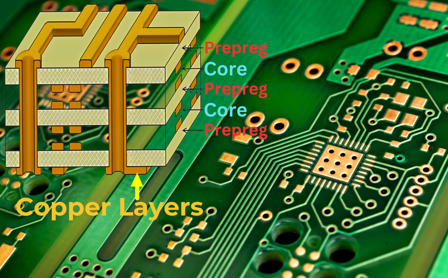
Blind vias are a type of via used in HDI PCB designs that connect an outer layer of the board to one or more inner layers without passing through the entire board. Unlike traditional through-hole vias, blind vias are "hidden" from the opposite side of the board, which saves space and allows for denser routing. This makes them a cornerstone of high density interconnect PCB technology, enabling smaller, lighter, and more efficient electronic devices.
In HDI designs, space is at a premium. Blind vias help by freeing up room on the board's surface, allowing for tighter component placement and shorter signal paths. This leads to improved signal integrity, with reduced noise and crosstalk—critical for high-speed applications operating at frequencies above 1 GHz. For instance, in a multilayer HDI board with 8 layers, blind vias can reduce the need for additional signal layers by up to 30%, optimizing both cost and performance.
Blind Via vs Microvia: Understanding the Difference
When discussing microvia vs blind via, it’s important to clarify their roles in HDI PCB designs. While the terms are sometimes used interchangeably, they are not identical. A blind via connects an outer layer to an inner layer without going through the entire board, as mentioned earlier. A microvia, on the other hand, is a smaller type of via—often with a diameter less than 150 micrometers (0.006 inches)—typically used in HDI designs to achieve fine pitch and high density.
In practice, most blind vias in HDI PCBs are also microvias due to their small size, created using laser drilling for precision. However, not all microvias are blind vias; some can be buried vias (connecting only inner layers) or through-hole vias in rare cases. The key takeaway is that microvias enable the miniaturization needed for HDI, while blind vias specifically address surface space constraints. For example, a typical microvia might have a diameter of 100 micrometers and a depth of 75 micrometers, ensuring a compact connection in tight spaces.
Choosing between these via types depends on your design needs. Blind vias are ideal for connecting surface-mounted components to inner signal layers, while microvias support finer geometries in densely packed areas.
Key Blind Via Layout Rules for HDI PCB Designs
Designing with blind vias requires careful attention to layout rules to ensure manufacturability and reliability. Following these blind via layout rules will help you avoid common pitfalls in HDI PCB blind via design and achieve a robust, high-performing board.
1. Maintain Proper Blind Via Aspect Ratio
The blind via aspect ratio—the ratio of the via’s depth to its diameter—is a critical factor in design and manufacturing. A high aspect ratio (e.g., greater than 1:1) can lead to issues like incomplete plating or structural weakness, increasing the risk of failure during thermal cycling. For most HDI designs, aim for an aspect ratio of 0.75:1 or lower. For instance, a blind via with a depth of 75 micrometers should have a diameter of at least 100 micrometers to maintain reliability.
Keeping the aspect ratio low ensures better copper plating inside the via, which is essential for electrical conductivity and thermal performance. Advanced manufacturing techniques, such as laser drilling, can achieve precise control over these dimensions, but always consult with your fabrication partner to confirm their capabilities.
2. Position Blind Vias Strategically
Place blind vias close to the components they connect to minimize signal path length. Shorter paths reduce signal loss and improve performance, especially in high-speed designs where signals can exceed 5 Gbps. However, avoid placing blind vias directly under sensitive components like BGAs (Ball Grid Arrays) unless using via-in-pad techniques, as this can complicate assembly and rework.
Additionally, distribute blind vias evenly across the board to prevent stress concentration during manufacturing processes like lamination. Uneven distribution can lead to board warpage, affecting the overall reliability of the PCB.
3. Adhere to Minimum Spacing Guidelines
In HDI layouts, spacing between vias and traces is tighter than in standard PCBs, but there are still limits. Ensure a minimum clearance of at least 150 micrometers (0.006 inches) between blind vias and adjacent traces or pads to prevent short circuits and manufacturing defects. For stacked or staggered via structures, maintain a spacing of at least 200 micrometers between via centers to avoid drilling inaccuracies.
These spacing rules are especially important in multilayer HDI designs with complex routing, where signal integrity can be compromised by crosstalk if vias are too close together.
4. Use Via-in-Pad for Maximum Density
Via-in-pad is a popular technique in HDI designs where blind vias are placed directly within the pads of surface-mounted components. This approach saves significant space, allowing for finer pitch components and denser layouts. However, it requires precise manufacturing and often involves filling the via with conductive or non-conductive material to create a flat surface for soldering. Ensure your design software accounts for via-in-pad requirements, and verify with your fabricator that they support this process.
Design Techniques for Optimizing Blind Via Performance
Beyond following blind via layout rules, adopting specific design techniques can enhance the performance of your high density interconnect PCB. These methods focus on signal integrity, thermal management, and manufacturability.
1. Optimize Signal Integrity with Blind Vias
Blind vias help shorten signal paths, which is a major advantage for high-speed designs. By connecting components directly to inner layers, you can reduce stub length—unwanted extensions of vias beyond the connected layer that cause signal reflection. For example, eliminating stubs in a 10 Gbps signal path can reduce signal reflection by up to 20%, improving overall performance.
To further enhance signal integrity, pair blind vias with controlled impedance traces. Maintain a consistent trace width (e.g., 4 mils for 50-ohm impedance) and use simulation tools to predict and mitigate potential issues like crosstalk or EMI (electromagnetic interference).
2. Manage Thermal Performance
Blind vias can also play a role in thermal management by connecting to inner copper planes that act as heat sinks. In high-power applications, ensure that blind vias are placed near heat-generating components to dissipate heat effectively. For instance, a blind via with a diameter of 120 micrometers can conduct heat away from a power IC, reducing junction temperature by as much as 5°C in some designs.
However, avoid overloading a single via with too much current, as this can lead to overheating. Distribute thermal vias across multiple points for balanced heat dissipation.
3. Leverage Stacked and Staggered Vias
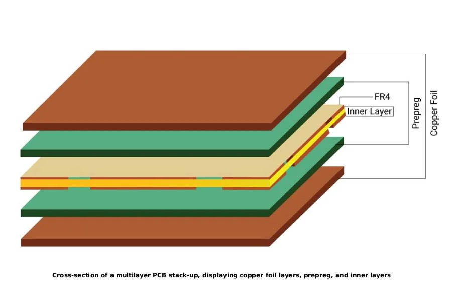
In complex HDI designs, stacked vias (blind vias placed directly on top of buried vias) and staggered vias (offset vias connecting adjacent layers) can maximize routing density. Stacked vias are ideal for connecting multiple layers in a compact area, while staggered vias reduce the risk of manufacturing defects by avoiding deep drilling in a single location. Both approaches require precise alignment, often within 50 micrometers, to ensure reliable connections.
Challenges in HDI PCB Blind Via Design and How to Overcome Them
While blind vias offer significant advantages, they also come with challenges that designers must address to ensure a successful HDI PCB blind via design.
1. Manufacturing Limitations
Blind vias, especially those with a small blind via aspect ratio, require advanced manufacturing techniques like laser drilling and sequential lamination. Not all fabricators can achieve the precision needed for microvias below 100 micrometers in diameter. To overcome this, collaborate closely with your manufacturing partner during the design phase to align your layout with their capabilities.
2. Cost Considerations
HDI designs with blind vias are often more expensive than standard PCBs due to the complexity of manufacturing. However, proper planning can mitigate costs. For example, reducing the number of layers by optimizing via placement can lower fabrication expenses by up to 15% without sacrificing performance.
3. Reliability Concerns
Smaller vias are more susceptible to defects like voids or cracks during thermal stress. To improve reliability, use high-quality materials with a low coefficient of thermal expansion (CTE), such as FR-4 with enhanced thermal properties, and conduct thorough testing like thermal cycling (e.g., -40°C to 85°C for 1000 cycles) to validate your design.
Conclusion: Mastering Blind Via Layout for Next-Level HDI Designs
Unlocking the full potential of high density interconnect PCB designs starts with mastering HDI PCB blind via design and adhering to blind via layout rules. By understanding the nuances of microvia vs blind via, maintaining an optimal blind via aspect ratio, and applying strategic design techniques, you can create compact, high-performance boards that meet the demands of modern electronics.
Whether you're designing for consumer gadgets, automotive systems, or telecommunications equipment, blind vias are a powerful tool to maximize PCB density. With careful planning and attention to detail, you can overcome the challenges of HDI design and deliver reliable, efficient, and cost-effective solutions.
Start implementing these best practices in your next project to see the difference that well-designed blind vias can make. Your journey to mastering HDI PCB layouts begins with a single via—make it count!
 ALLPCB


