If you're facing issues with solder-related problems in Surface Mount Technology (SMT) assembly for your printed circuit boards (PCBs), you're not alone. Common challenges like solder bridging, tombstoning, and insufficient solder can disrupt production and affect product reliability. In this comprehensive guide, we'll dive deep into troubleshooting these solder SMT problems, offering practical solutions to ensure a smooth SMT assembly process for your PCB projects. Whether you're an engineer or a hobbyist, this blog will equip you with actionable insights to tackle these issues head-on.
What Are Solder-Related SMT Assembly Problems?
SMT assembly is a critical process in modern electronics manufacturing, where components are mounted directly onto the surface of a PCB. While this method offers advantages like compact design and high-speed production, solder-related issues can arise due to various factors such as incorrect soldering techniques, poor design, or suboptimal materials. These problems can lead to defective boards, costly rework, and delayed timelines. Let's explore the most common solder SMT problems and how to address them effectively during PCB assembly.
Common Solder-Related Issues in SMT Assembly
Understanding the root causes of solder issues is the first step to troubleshooting. Below are some of the most frequent problems encountered during SMT assembly, along with their causes and symptoms.
1. Solder Bridging
Solder bridging occurs when excess solder creates an unintended connection between two or more pads or leads on a PCB. This can cause short circuits, leading to malfunctioning circuits. Solder bridging is often visible as a small blob of solder connecting adjacent pins or pads.
Causes:
- Excessive solder paste application during the printing process.
- Incorrect stencil design, leading to uneven paste distribution.
- Improper component placement, causing pads to be too close together.
- Reflow oven temperature profiles that are too high, causing solder to flow uncontrollably.
Solution:
- Adjust the stencil design to ensure precise solder paste application, targeting a thickness of about 0.1 to 0.15 mm for most SMT components.
- Use a solder paste inspection (SPI) system to detect over-application before reflow.
- Optimize the reflow profile, maintaining a peak temperature between 235°C and 250°C for lead-free solder to prevent excessive flow.
- Ensure proper component spacing in the PCB layout to avoid overlap.
2. Tombstoning
Tombstoning is a defect where one end of a passive component, like a resistor or capacitor, lifts off the PCB during reflow soldering, resembling a tombstone. This issue disrupts the electrical connection and can compromise the board's functionality.
Causes:
- Uneven heating during reflow, causing one pad to solidify before the other.
- Imbalanced pad sizes or shapes, leading to uneven solder wetting.
- Excessive solder paste on one pad compared to the other.
- Component misalignment during placement.
Solution:
- Ensure uniform pad design in your PCB layout, maintaining equal size and shape for both ends of passive components.
- Balance the reflow oven temperature profile with a gradual ramp-up rate of 1.5°C to 2.5°C per second to avoid thermal shock.
- Use automated optical inspection (AOI) systems post-placement to detect misaligned components before reflow.
- Apply consistent solder paste volume, targeting a stencil aperture that matches the pad size.
3. Insufficient Solder
Insufficient solder results in weak or incomplete joints, leading to poor electrical connections and potential failures over time. This issue often appears as joints that look dull or have visible gaps between the component lead and pad.
Causes:
- Inadequate solder paste volume during printing.
- Poor stencil alignment, causing paste to miss the pads.
- Oxidation on pads or component leads, preventing proper solder wetting.
- Low reflow temperature, failing to melt solder completely.
Solution:
- Verify stencil alignment and cleanliness before printing to ensure accurate paste deposition.
- Use a reflow temperature profile with a peak of at least 235°C for lead-free solder to ensure complete melting.
- Clean PCB pads and component leads to remove oxidation, using a flux if necessary.
- Measure solder paste volume with an SPI tool, aiming for 80-90% pad coverage for optimal wetting.
4. Cold Solder Joints
Cold solder joints occur when the solder doesn't fully melt or bond with the pad and component lead, resulting in a weak, unreliable connection. These joints often look grainy or dull instead of shiny and smooth.
Causes:
- Insufficient heat during reflow, often below 220°C for lead-free solder.
- Rapid cooling after reflow, preventing proper crystallization of the solder joint.
- Contamination on pads or leads, hindering solder adhesion.
Solution:
- Adjust the reflow profile to maintain a time above liquidus (TAL) of 60-90 seconds for lead-free solder.
- Ensure a controlled cooling rate of 2-4°C per second after reflow to allow proper joint formation.
- Use high-quality flux to clean surfaces and improve solder wetting during the process.
Best Practices for Preventing Solder SMT Problems
While troubleshooting is essential, preventing solder-related issues in SMT assembly can save time and resources. Here are some proven strategies to minimize defects during PCB production.
1. Optimize PCB Design for Manufacturability
A well-thought-out PCB design can prevent many solder-related issues. Ensure pad sizes match component specifications, typically ranging from 0.2 mm to 0.5 mm larger than the component lead for proper solder fillet formation. Maintain a minimum spacing of 0.2 mm between pads to avoid bridging. Additionally, include fiducial marks for precise component placement during assembly.
2. Use High-Quality Materials
The quality of solder paste, flux, and PCB surface finish plays a significant role in SMT assembly success. Opt for a Type 3 or Type 4 solder paste with a particle size of 25-45 microns for fine-pitch components. Choose a surface finish like ENIG (Electroless Nickel Immersion Gold) for better solderability and resistance to oxidation.
3. Calibrate Reflow Oven Profiles
A well-calibrated reflow oven profile is critical for consistent soldering. Follow these general guidelines for lead-free solder:
- Preheat Zone: Ramp up at 1.5-2.5°C per second to 150-180°C.
- Soak Zone: Hold at 180-200°C for 60-120 seconds to activate flux.
- Reflow Zone: Peak at 235-250°C for 20-40 seconds.
- Cooling Zone: Cool at 2-4°C per second to room temperature.
Regularly test the profile using a thermal profiler to ensure accuracy across the board.
4. Implement Inspection Systems
Automated inspection tools like SPI and AOI can catch issues early in the SMT assembly process. SPI checks solder paste volume and alignment post-printing, while AOI verifies component placement and solder joint quality after reflow. These systems can reduce defect rates by up to 70%, according to industry studies.
Advanced Troubleshooting Tips for SMT Assembly
For complex or recurring solder SMT problems, consider these advanced troubleshooting techniques to pinpoint and resolve issues.
1. Use X-Ray Inspection for Hidden Joints
For components like Ball Grid Arrays (BGAs) where solder joints are hidden under the package, X-ray inspection can reveal defects such as voids or insufficient solder. Voids larger than 25% of the joint area can weaken connections, so aim for minimal voiding by optimizing reflow profiles and paste application.
2. Analyze Solder Joint Microstructure
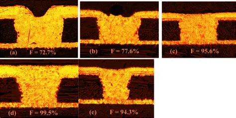
If failures persist, conduct a cross-sectional analysis of solder joints using a microscope. Look for intermetallic compound (IMC) layer thickness, which should ideally be 1-5 microns for a reliable joint. Excessive IMC growth can indicate overheating or prolonged reflow times, requiring profile adjustments.
3. Test for Thermal Stress
Thermal cycling tests can uncover latent solder joint issues. Subject the PCB to temperature cycles between -40°C and 85°C for 500-1000 cycles, then inspect for cracks or delamination. This can help identify weak joints caused by mismatched coefficients of thermal expansion (CTE) between components and the board.
How to Handle Rework for Solder SMT Problems
When defects occur, rework is often necessary to salvage the PCB. Follow these steps for effective rework without damaging the board or components.
1. Remove Defective Components
Use a hot air rework station set to 300-350°C to gently heat the area around the defective component. Once the solder melts, lift the component with tweezers. Avoid excessive heat to prevent pad damage or board delamination.
2. Clean the Area
After removal, clean the pads with a desoldering braid and isopropyl alcohol to remove old solder and flux residue. Ensure the pads are flat and free of debris before proceeding.
3. Reapply Solder and Place Component
Apply fresh solder paste or flux to the pads, then place the new component using precision tweezers. Use the hot air station again to reflow the solder, ensuring a shiny, even joint.
Conclusion: Mastering SMT Assembly for Reliable PCBs
Troubleshooting solder-related SMT assembly problems is a vital skill for achieving high-quality PCB production. By understanding common issues like solder bridging, tombstoning, insufficient solder, and cold joints, and by implementing preventive measures such as optimized design, quality materials, and precise reflow profiles, you can significantly reduce defects. Advanced techniques like X-ray inspection and thermal testing further ensure reliability for complex projects. With these strategies, you're well-equipped to tackle solder SMT problems and streamline your SMT assembly process for flawless PCB outcomes.
At ALLPCB, we're committed to supporting your electronics manufacturing journey with expert resources and services tailored to your needs. Keep these tips in mind for your next project, and watch your assembly success rate soar!
 ALLPCB


