 ALLPCB


If you're facing a solder mask peeling or chipping issue on your PCB, you're likely dealing with a frustrating problem that can compromise the integrity and functionality of your board. This issue often stems from improper surface preparation, incorrect curing processes, or material mismatches during manufacturing. In this comprehensive guide, we'll dive deep into the causes of solder mask peeling and chipping, a common PCB design issue, and provide actionable solutions to help you resolve this PCB problem effectively.
What Is Solder Mask Peeling and Chipping on a PCB?
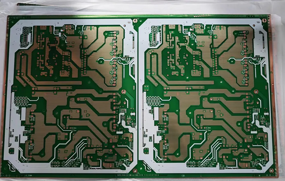
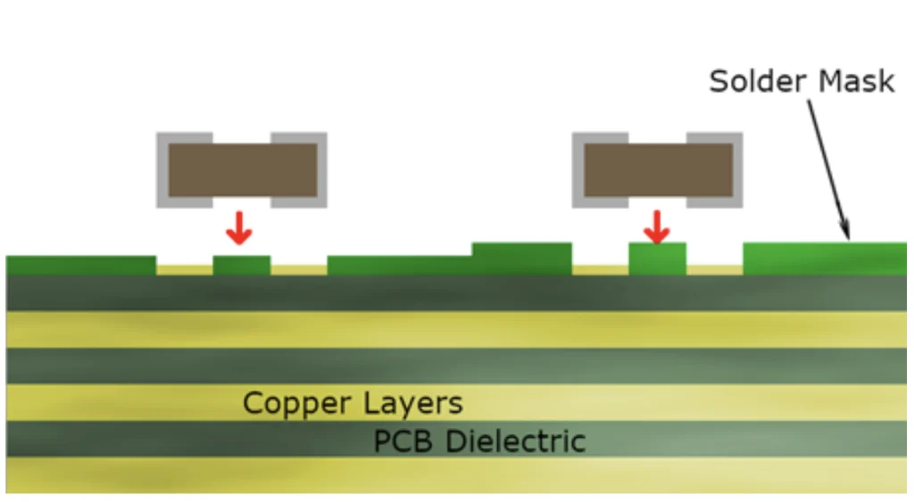
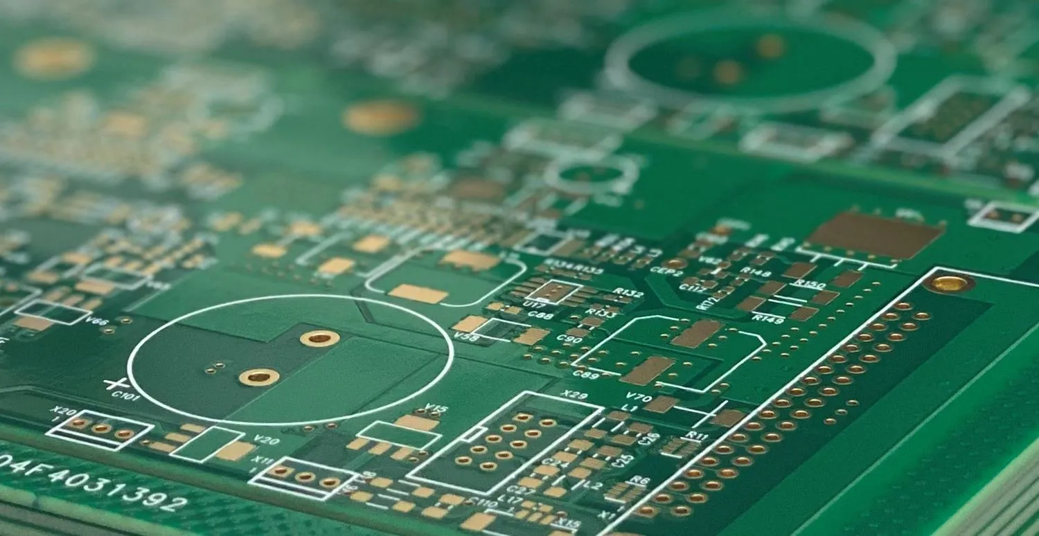
The solder mask is a thin protective layer applied to the surface of a printed circuit board (PCB) to insulate copper traces, prevent solder bridges during assembly, and shield the board from environmental factors like moisture and oxidation. When the solder mask starts peeling or chipping, it exposes the underlying copper, leading to potential shorts, corrosion, or assembly failures. This PCB problem can occur during manufacturing, soldering, or even after the board is in use, making it a critical issue to address for reliable performance.
In the following sections, we'll break down the root causes of solder mask peeling, explore how it impacts PCB design, and offer practical troubleshooting steps to fix and prevent this issue.
Why Does Solder Mask Peeling and Chipping Happen?
Understanding the reasons behind solder mask peeling and chipping is the first step in troubleshooting this PCB design issue. Several factors during the manufacturing process or usage can contribute to this problem. Let's explore the most common causes:
1. Poor Surface Preparation
Before applying the solder mask, the PCB surface must be thoroughly cleaned to remove contaminants like oils, dust, or oxidation. If the surface isn't properly prepared, the solder mask may not adhere well to the copper, leading to peeling or chipping over time. For instance, residual flux or grease can create a barrier that prevents proper bonding, causing adhesion failures.
2. Incorrect Curing Process
The solder mask needs to be cured at specific temperatures and durations to achieve optimal adhesion and durability. If the curing temperature is too low (e.g., below the recommended 120-150°C for most liquid photoimageable masks) or the curing time is insufficient, the mask may not fully harden, making it prone to chipping. Conversely, over-curing at excessively high temperatures (e.g., above 160°C for extended periods) can cause brittleness, leading to cracks and peeling.
3. Material Mismatch
Not all solder mask materials are compatible with every PCB substrate or manufacturing process. For example, using a solder mask with a different thermal expansion coefficient than the PCB material can cause stress during temperature changes, leading to peeling. This is especially common in high-temperature applications where the board undergoes repeated thermal cycling.
4. Mechanical Stress During Assembly
During PCB assembly, components are soldered onto the board, often involving high temperatures and mechanical handling. If the solder mask is not robust enough to withstand the stress of soldering (e.g., wave soldering at 260°C), or if tools and fixtures scratch the surface, chipping can occur. This is a frequent PCB problem in automated assembly lines with improper handling.
5. Environmental Factors
After assembly, PCBs are often exposed to harsh environments, including humidity, temperature fluctuations, and chemical exposure. These conditions can degrade the solder mask over time, causing it to peel or chip. For example, prolonged exposure to moisture levels above 85% relative humidity can weaken the mask's adhesion, especially if it wasn't sealed properly during manufacturing.
Impact of Solder Mask Peeling on PCB Performance
Solder mask peeling and chipping aren't just cosmetic issues; they can severely impact the functionality and reliability of a PCB. Here's how this PCB design issue affects your board:
- Exposed Copper Traces: When the solder mask peels off, copper traces are exposed to air and moisture, leading to oxidation and corrosion. This can increase resistance or cause open circuits, disrupting signal integrity.
- Solder Bridges: Without a protective layer, solder can unintentionally flow between adjacent pads during assembly, creating shorts that cause malfunctions.
- Reduced Lifespan: Environmental damage from peeling accelerates wear and tear on the PCB, shortening its operational life.
- Assembly Failures: Chipped areas can interfere with component placement or soldering, leading to poor connections and rework costs.
Addressing solder mask peeling early is crucial to avoid these costly and time-consuming issues in your PCB design.
Troubleshooting Solder Mask Peeling and Chipping Issues
Now that we understand the causes and impacts of this PCB problem, let's walk through a step-by-step troubleshooting process to identify and resolve solder mask peeling and chipping in your boards.
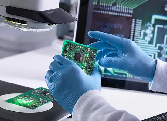
Step 1: Inspect the PCB for Visible Damage
Start by visually inspecting the PCB under good lighting or with a magnifying tool. Look for areas where the solder mask has lifted, cracked, or chipped away. Pay close attention to high-stress areas like edges, corners, and near solder pads. Document the extent of the damage and note whether it appears during manufacturing, assembly, or after environmental exposure.
Step 2: Review Manufacturing Processes
Check the manufacturing records or consult with your production team to evaluate the processes used during solder mask application. Key points to verify include:
- Was the PCB surface cleaned properly before applying the solder mask? Ensure no contaminants were present.
- Were the curing temperature and time within the recommended range for the specific solder mask material (e.g., 120-150°C for 20-30 minutes for most liquid masks)?
- Was the correct type of solder mask used for the PCB material and application?
If any deviations are found, they could be the root cause of the peeling issue.
Step 3: Test for Adhesion Strength
Perform an adhesion test to assess how well the solder mask sticks to the PCB surface. A common method is the tape test, where a piece of adhesive tape is pressed onto the solder mask and then peeled off. If the mask comes off with the tape, adhesion is poor, indicating a problem with surface preparation or curing. Industry standards often require the mask to withstand a pull force of at least 5 N/cm without delaminating.
Step 4: Evaluate Environmental Conditions
If the peeling occurs after assembly or during use, assess the environmental conditions the PCB has been exposed to. Measure factors like humidity (should be below 85% for most applications), temperature ranges (e.g., -40°C to 85°C for standard boards), and exposure to chemicals. If conditions exceed the PCB's design limits, consider using a more durable solder mask or adding conformal coating for extra protection.
Step 5: Analyze Mechanical Stress Points
Examine the assembly process to identify potential sources of mechanical stress. Check if tools, fixtures, or automated equipment are scratching or damaging the solder mask. Also, review soldering temperatures (e.g., peak reflow temperatures should not exceed 260°C for most masks) to ensure they aren't causing thermal shock to the mask layer.
Solutions to Prevent Solder Mask Peeling and Chipping
Once you've identified the cause of the solder mask peeling or chipping, implement these solutions to fix the current issue and prevent it from happening in future PCB designs.
1. Optimize Surface Preparation
Ensure the PCB surface is meticulously cleaned before solder mask application. Use chemical cleaning agents or micro-etching processes to remove oxides and contaminants. A clean surface roughness of about 1-2 μm is often ideal for good adhesion. Regularly maintain cleaning equipment to avoid introducing new contaminants during production.
2. Fine-Tune the Curing Process
Adhere strictly to the manufacturer’s curing guidelines for the solder mask material. Use calibrated ovens to maintain consistent temperatures (e.g., 130°C for 25 minutes for many standard masks). Avoid rapid cooling after curing, as thermal shock can weaken the mask. Gradual cooling over 10-15 minutes can help reduce internal stress.
3. Select Compatible Materials
Choose a solder mask that matches the thermal and mechanical properties of your PCB substrate. For high-temperature applications, consider using a mask with a higher glass transition temperature (Tg), such as 140°C or above, to withstand thermal cycling without cracking or peeling.
4. Minimize Mechanical Stress
Adjust assembly processes to reduce physical stress on the PCB. Use protective fixtures during handling and ensure soldering profiles are within safe limits (e.g., preheat at 100-120°C for 60-90 seconds before reflow). Train staff to handle boards carefully to avoid scratches or impacts that could chip the mask.
5. Enhance Environmental Protection
For PCBs exposed to harsh conditions, apply an additional conformal coating after assembly to provide an extra layer of protection against moisture and chemicals. Select a coating with good adhesion to the solder mask (e.g., acrylic or silicone-based coatings) and ensure it’s compatible with the board’s operating environment.
Best Practices for PCB Design to Avoid Solder Mask Issues
Preventing solder mask peeling starts at the design stage. Incorporate these best practices into your PCB design process to minimize the risk of this common PCB problem:
- Adequate Clearance: Design solder mask openings with sufficient clearance around pads (e.g., 0.05-0.1 mm larger than the pad size) to avoid stress concentration during soldering.
- Via Tenting: Ensure vias are properly tented or plugged to prevent solder mask thinning in those areas, which can lead to peeling.
- Uniform Thickness: Specify a uniform solder mask thickness (typically 0.8-1.2 mils) to avoid weak spots prone to chipping.
- Thermal Considerations: Account for thermal expansion in your design by selecting materials with similar coefficients of thermal expansion (CTE) to reduce stress during temperature changes.
Conclusion
Solder mask peeling and chipping is a significant PCB design issue that can lead to costly failures if not addressed promptly. By understanding the root causes—such as poor surface preparation, incorrect curing, or environmental stress—you can take proactive steps to troubleshoot and resolve this PCB problem. Implementing solutions like optimizing manufacturing processes, selecting compatible materials, and following design best practices will help ensure your boards remain reliable and durable.
At ALLPCB, we’re committed to helping you achieve high-quality PCB production. Whether you're dealing with solder mask peeling or other manufacturing challenges, our expertise and resources are here to support you in creating robust and efficient designs. Keep these tips in mind for your next project to avoid common pitfalls and enhance the performance of your PCBs.


