If you're looking for a way to achieve high-precision results in high-layer-count PCB manufacturing, Laser Direct Imaging (LDI) offers unmatched benefits. This advanced technology eliminates traditional photomasks, boosts accuracy, and supports the production of complex, dense circuit boards with fine lines and tight tolerances. In this blog, we’ll dive deep into why LDI is a game-changer for PCB production, especially for intricate designs, and explore its specific advantages with detailed insights.
What Is Laser Direct Imaging (LDI) in PCB Manufacturing?
Laser Direct Imaging, or LDI, is a cutting-edge photolithography technique used in PCB manufacturing. Unlike traditional methods that rely on physical photomasks to transfer circuit patterns onto a board, LDI uses a computer-controlled laser to directly expose photosensitive materials on the PCB substrate. This results in highly precise imaging, making it ideal for high-layer-count and high-density interconnect (HDI) designs.
With LDI, manufacturers can achieve resolutions down to sub-micron levels, often as fine as 10 micrometers for line widths and spacing. This level of precision is critical for modern electronics, where components are shrinking, and boards must accommodate more layers—sometimes exceeding 20 layers in advanced applications like telecommunications or medical devices.
Why High-Layer-Count PCBs Need Precision
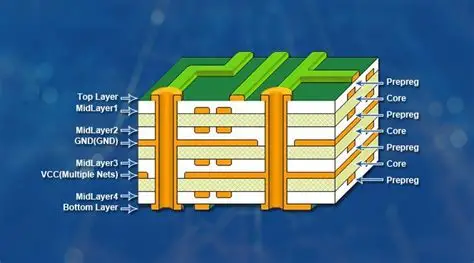
High-layer-count PCBs, often containing 10 to 30 layers or more, are essential for complex electronic systems. These boards are used in industries like aerospace, automotive, and 5G technology, where signal integrity and space efficiency are paramount. However, as the number of layers increases, so does the challenge of maintaining alignment and precision across each layer.
For example, a 24-layer PCB used in a server motherboard may require impedance control within ±5% to ensure signal speeds remain consistent at high frequencies, often exceeding 10 GHz. Even a slight misalignment of 5 micrometers between layers can cause signal degradation or crosstalk. Traditional imaging methods struggle to meet these tight tolerances, which is where LDI shines.
Key Advantages of Laser Direct Imaging in High-Layer-Count PCB Manufacturing
Let’s explore the specific benefits of using LDI for high-layer-count PCB production. Each advantage contributes to better quality, efficiency, and reliability in manufacturing.
1. Unparalleled Precision for Fine Lines and Tight Tolerances
LDI achieves exceptional accuracy by using a focused laser beam to directly write circuit patterns. This eliminates errors caused by photomask misalignment or wear, which are common in traditional processes. With LDI, manufacturers can consistently produce line widths and spacing as small as 10-15 micrometers, critical for HDI designs in high-layer-count boards.
This precision is especially important for maintaining signal integrity in multi-layer PCBs, where even tiny deviations can disrupt performance. For instance, in a 5G base station PCB with 20 layers, LDI ensures that microvias (small vias connecting layers) are perfectly aligned, reducing signal loss and improving reliability.
2. Improved Registration Accuracy Across Multiple Layers
In high-layer-count PCBs, registration—the alignment of layers—must be flawless. A misalignment of just a few micrometers can lead to connection failures or short circuits. LDI uses digital data to control the laser, ensuring layer-to-layer alignment accuracy within ±2 micrometers, far superior to traditional methods that often vary by ±10 micrometers or more.
This capability is vital for stacked vias and buried vias in boards with 16 or more layers. For example, in automotive radar systems, precise registration ensures that high-frequency signals (often around 77 GHz) travel without interference, maintaining the system’s accuracy.
3. Elimination of Photomasks for Cost and Time Savings
Traditional PCB imaging requires creating and maintaining physical photomasks for each design, which is both time-consuming and expensive, especially for prototypes or small-batch runs. LDI bypasses this step by directly imaging from digital files, reducing production lead times by up to 50% in some cases.
For high-layer-count PCBs, where multiple masks are needed, the cost savings are significant. Additionally, eliminating photomasks reduces the risk of defects caused by mask damage or dust particles, further improving yield rates.
4. Flexibility for Complex and Custom Designs
High-layer-count PCBs often feature unique layouts tailored to specific applications, such as flexible-rigid boards or designs with embedded components. LDI’s digital nature allows for quick design changes without the need to produce new masks, making it ideal for rapid prototyping and customization.
For instance, in medical devices like MRI machines, where PCBs may need 18 layers with varying trace patterns, LDI can adapt to last-minute design tweaks, ensuring the project stays on schedule without compromising precision.
5. Enhanced Capability for High-Density Interconnect (HDI) Boards
HDI technology is a cornerstone of modern high-layer-count PCBs, enabling more components to fit into smaller spaces. LDI supports HDI by providing the precision needed for microvias (diameters as small as 50 micrometers) and ultra-fine traces. This is crucial for applications like smartphones or wearable devices, where board space is limited, yet performance demands are high.
With LDI, manufacturers can achieve via-in-pad designs and stacked microvias across multiple layers without risking misalignment, ensuring reliable connections in dense layouts.
6. Reduced Defects and Higher Yield Rates
Defects in high-layer-count PCBs can be catastrophic, leading to costly rework or product failures. LDI minimizes defects by avoiding issues like photomask scratches or misalignment. Studies suggest that LDI can improve first-pass yield rates by up to 20% compared to traditional methods, saving time and resources in large-scale production.
For example, in aerospace applications where a 30-layer PCB controls critical navigation systems, LDI’s defect reduction ensures that every board meets stringent reliability standards.
7. Environmentally Friendly Process
LDI is a greener alternative to traditional imaging. By eliminating the need for photomasks and reducing chemical waste associated with mask production, it lowers the environmental impact of PCB manufacturing. This is increasingly important as industries move toward sustainable practices, and it can help companies meet regulatory requirements for eco-friendly production.
Applications of LDI in High-Layer-Count PCB Manufacturing
The advantages of LDI make it a preferred choice for various industries that rely on high-layer-count PCBs. Here are some key applications where this technology excels:
- Telecommunications: 5G infrastructure requires PCBs with 20+ layers to handle high-frequency signals (up to 28 GHz or more). LDI ensures precise trace widths and via placement for optimal performance.
- Automotive: Advanced driver-assistance systems (ADAS) use multi-layer boards for sensors and radar. LDI’s precision supports reliable signal transmission at frequencies like 77 GHz.
- Medical Devices: Equipment like CT scanners often uses 18-24 layer PCBs. LDI enables the fine pitch and tight tolerances needed for compact, high-performance designs.
- Aerospace and Defense: High-layer-count PCBs in satellites or avionics demand zero defects. LDI’s accuracy and repeatability are critical for mission-critical systems.
Challenges and Considerations with LDI
While LDI offers numerous benefits, it’s important to understand its limitations. The initial investment in LDI equipment can be high, which may pose a barrier for smaller manufacturers. Additionally, the process requires skilled operators to manage the digital systems and maintain the laser equipment for consistent results.
However, for high-layer-count PCB production, the long-term cost savings, improved quality, and faster turnaround times often outweigh these challenges, making LDI a worthwhile investment for manufacturers focused on precision and scalability.
How LDI Enhances Your PCB Manufacturing Process
Integrating LDI into your PCB manufacturing workflow can transform the way you produce high-layer-count boards. By leveraging digital imaging, you gain the ability to handle complex designs with ease, reduce production errors, and meet the tight tolerances required for modern electronics. Whether you’re working on HDI boards for consumer gadgets or multi-layer PCBs for industrial systems, LDI provides the precision and flexibility needed to stay competitive.
At ALLPCB, we understand the importance of adopting advanced technologies like LDI to deliver top-quality results. Our focus is on providing high-precision PCB solutions that meet the demands of today’s fast-paced industries, ensuring your projects are completed with accuracy and efficiency.
Conclusion
Laser Direct Imaging (LDI) is revolutionizing high-layer-count PCB manufacturing by offering unmatched precision, flexibility, and efficiency. From achieving fine line resolutions of 10 micrometers to ensuring perfect layer registration in 30-layer boards, LDI addresses the challenges of producing complex, high-density designs. Its ability to eliminate photomasks, reduce defects, and support HDI technology makes it an invaluable tool for industries ranging from telecommunications to aerospace.
By adopting LDI, manufacturers can not only improve the quality of their PCBs but also streamline production and adapt to evolving design needs. As the demand for smaller, faster, and more reliable electronics continues to grow, LDI stands out as the future of high-precision PCB manufacturing.
 ALLPCB


