ALLPCB


If you're looking to understand the stacked via PCB manufacturing process, you've come to the right place. Stacked vias are critical in high-density interconnect (HDI) designs, allowing for compact, multi-layered printed circuit boards (PCBs) used in advanced electronics. This guide dives deep into the key steps like sequential lamination, laser drilling for PCBs, and copper plating for vias, while also addressing common PCB manufacturing defects and the importance of quality control in PCB manufacturing. Whether you're an engineer or a designer, you'll find actionable insights to navigate the complexities of this process.
In the sections below, we'll explore each stage of manufacturing stacked via PCBs, highlight the challenges, and provide practical tips to ensure high-quality results. Let's get started with the fundamentals and build a clear understanding of this intricate process.
What Are Stacked Vias and Why Are They Important in PCB Design?
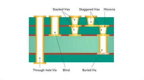
Stacked vias are vertical interconnects in a PCB that are placed directly on top of each other, connecting multiple layers in a compact space. Unlike staggered vias, which are offset, stacked vias save space and are essential for HDI PCBs used in smartphones, tablets, and other small, high-performance devices. They allow for denser routing and better signal integrity, often supporting frequencies up to several GHz in high-speed designs.
The importance of stacked vias lies in their ability to reduce the PCB footprint while maintaining functionality. For example, in a 10-layer HDI board, stacked vias can connect layers 1 to 3 and 3 to 5 directly, minimizing signal path length and reducing impedance mismatches, which can be as critical as maintaining 50 ohms for specific high-speed signals. However, manufacturing these vias comes with unique challenges that require precision and advanced techniques.
The Stacked Via PCB Manufacturing Process: Step-by-Step
The manufacturing of stacked via PCBs involves several specialized steps to ensure reliability and performance. Below, we break down the key processes involved, focusing on precision and the technologies that make HDI designs possible.
1. Design and Pre-Production Planning
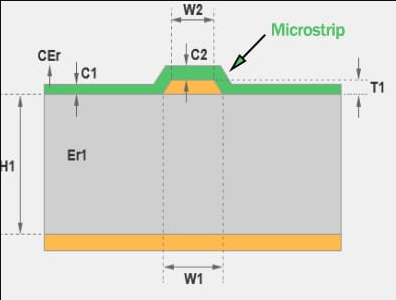
Before manufacturing begins, the PCB design must be finalized with detailed specifications for via placement, layer stack-up, and impedance requirements. Software tools are used to simulate signal integrity and ensure that stacked vias align perfectly across layers. Misalignment by even 0.05 mm can lead to connection failures, so precision at this stage is critical.
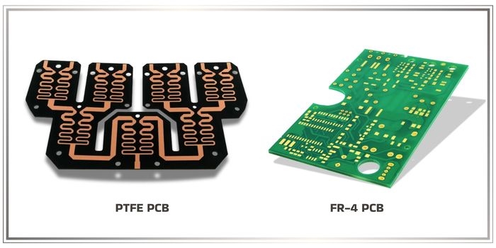
During pre-production, manufacturers select materials like FR-4 or high-frequency laminates based on the project's needs. Dielectric thickness, often as thin as 0.1 mm in HDI designs, is also determined to control impedance and signal speed.
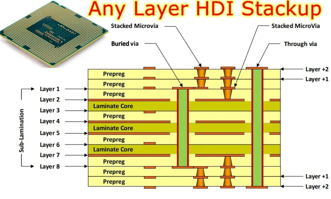
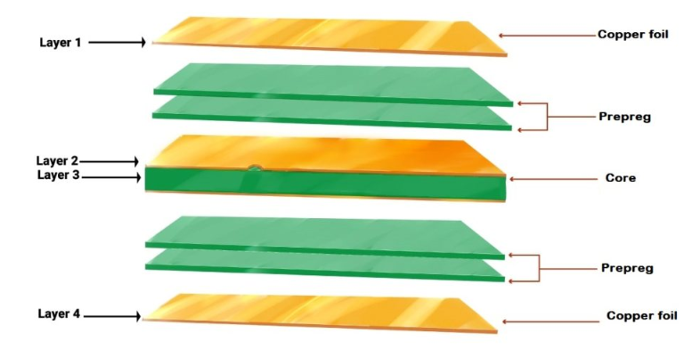
2. Sequential Lamination for Multi-Layer Builds
Sequential lamination is a core process in creating HDI PCBs with stacked vias. Unlike traditional lamination, where all layers are pressed together at once, sequential lamination builds the board in stages. Subsets of layers are laminated, drilled, and plated before additional layers are added. This method allows for the creation of buried and blind vias, which are often stacked to save space.
For instance, a 12-layer PCB might be built in three lamination cycles, with vias drilled and plated after each cycle. This process ensures precise alignment but increases manufacturing time and cost. Maintaining uniform pressure (around 300-400 psi) and temperature (approximately 180°C) during lamination is vital to avoid delamination or warping.
3. Laser Drilling for PCBs: Precision in Via Creation
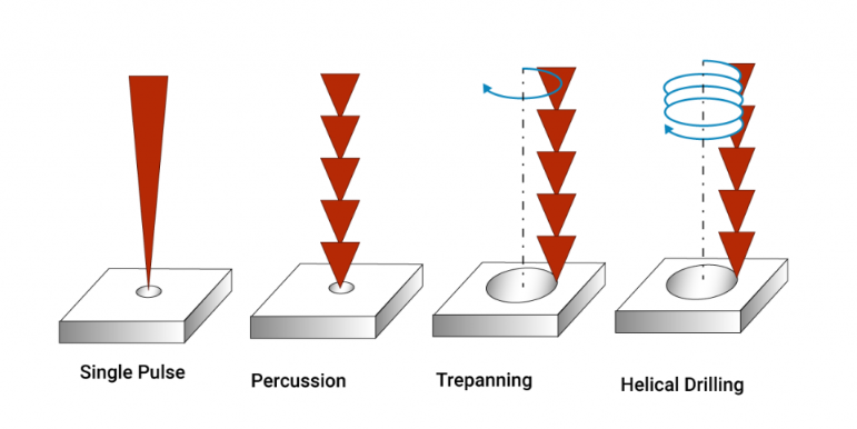
Laser drilling is the go-to method for creating microvias in HDI PCBs, especially for stacked vias with diameters as small as 0.1 mm. Unlike mechanical drilling, which is better suited for larger through-holes, laser drilling offers high precision and can target specific depths for blind and buried vias.
The process uses a focused UV or CO2 laser to ablate the dielectric material, creating clean, tapered holes. However, controlling the laser's energy is crucial—too much heat can damage surrounding copper or cause resin smear, leading to poor plating. Modern systems can achieve drilling speeds of up to 1000 vias per minute, but accuracy remains the priority over speed.
4. Copper Plating for Vias: Ensuring Reliable Connections
After drilling, the vias must be plated with copper to establish electrical connectivity between layers. Copper plating for vias involves a multi-step process, starting with cleaning the via walls to remove debris and resin smear. This is followed by electroless copper deposition, which creates a thin conductive layer, and then electrolytic plating to build up the copper thickness to around 20-25 microns for standard designs.
In stacked vias, uniform plating is challenging due to the small diameter and high aspect ratio (depth-to-diameter ratio, often 1:1 or higher). Incomplete plating can result in weak connections or open circuits, especially in high-current applications where vias must handle up to 2-3 amps. Advanced plating chemistries and pulse-reverse techniques are often used to ensure even copper distribution.
5. Final Assembly and Testing
Once the vias are plated and all layers are laminated, the PCB undergoes final routing, solder mask application, and surface finishing (like ENIG or HASL). Testing is a critical step to verify the integrity of stacked vias. Techniques like Automated Optical Inspection (AOI) and X-ray imaging are used to check for misalignment or plating defects, ensuring that signal paths maintain integrity at high frequencies, such as 5 GHz for modern communication devices.
Common Challenges in Stacked Via PCB Manufacturing
While stacked vias enable compact and high-performance designs, their manufacturing process is fraught with challenges. Understanding these issues can help in mitigating risks and improving outcomes.
1. Alignment Issues in Sequential Lamination
Since sequential lamination builds the PCB in stages, maintaining alignment between layers is a significant challenge. A misalignment of just 0.025 mm can cause stacked vias to fail, leading to broken connections. Advanced registration systems and fiducial markers are used to improve accuracy, but even slight thermal expansion during lamination (often 0.01% per degree Celsius) can introduce errors.
2. Defects in Laser Drilling and Copper Plating
Laser drilling, while precise, can lead to defects like taper variation or incomplete material removal, affecting via quality. Similarly, copper plating for vias can result in voids or uneven thickness, especially in high-aspect-ratio vias. These PCB manufacturing defects can cause signal loss or reliability issues, particularly in applications requiring impedance control within ±5% tolerance.
3. Thermal and Mechanical Stress
Stacked vias are prone to thermal and mechanical stress during operation. Temperature cycling (e.g., -40°C to 85°C in automotive applications) can cause cracks in the copper plating due to differences in thermal expansion between materials. Ensuring robust design rules, such as maintaining a minimum via wall thickness of 20 microns, helps mitigate these risks.
Quality Control in PCB Manufacturing: Ensuring Reliable Stacked Vias
Quality control in PCB manufacturing is non-negotiable when dealing with stacked vias. A single defect can compromise an entire board, leading to costly rework or product failures. Here are the key strategies to ensure high-quality outcomes.
1. Rigorous Inspection Techniques
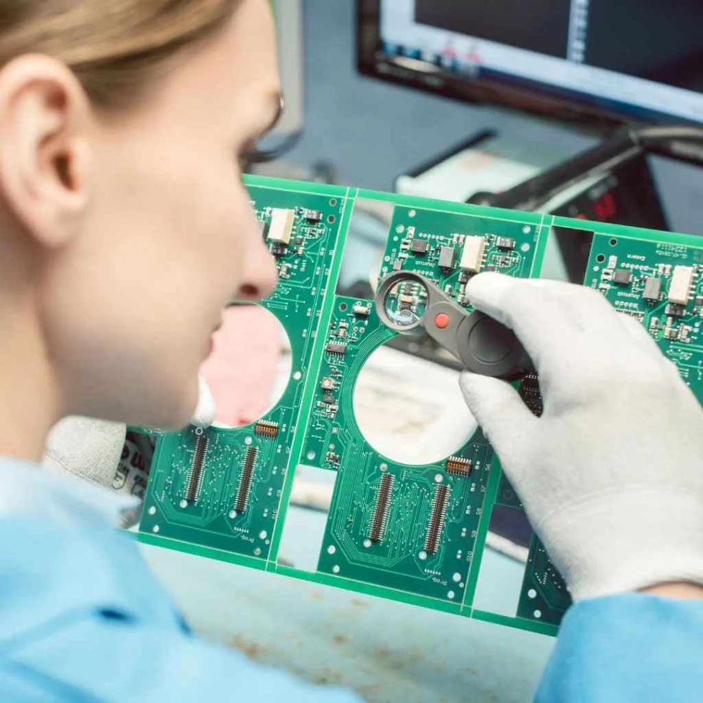
Manufacturers employ multiple inspection methods to catch defects early. X-ray inspection can detect hidden voids in copper plating, while AOI systems scan for surface-level misalignment or drilling errors. For critical applications, microsectioning—cutting and examining a sample PCB under a microscope—is used to verify via integrity.
2. Process Monitoring and Control
Every stage, from laser drilling to copper plating, must be tightly controlled. For example, maintaining a consistent laser power output (within ±2%) prevents over-drilling, while monitoring plating bath chemistry ensures uniform copper deposition. Statistical Process Control (SPC) is often used to track variations and maintain process stability.
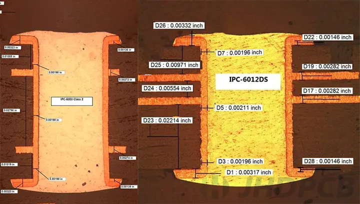
3. Compliance with Industry Standards
Adhering to standards like IPC-6012 (Qualification and Performance Specification for Rigid PCBs) ensures that stacked via PCBs meet reliability and performance benchmarks. For instance, IPC Class 3 standards for high-reliability applications mandate stricter tolerances for via plating thickness and alignment compared to consumer-grade Class 2 boards.
Tips for Designing and Manufacturing Stacked Via PCBs
To achieve successful outcomes with stacked via PCBs, consider the following practical tips during design and manufacturing:
- Optimize Via Placement: Avoid placing stacked vias too close to high-stress areas like board edges, as this increases the risk of cracking under mechanical stress.
- Specify Material Properties: Choose dielectric materials with low thermal expansion coefficients (e.g., below 15 ppm/°C) to minimize alignment issues during lamination.
- Collaborate with Manufacturers: Work closely with your fabrication partner to define achievable tolerances for drilling and plating, especially for vias smaller than 0.15 mm in diameter.
- Test Early and Often: Incorporate test points in your design to allow for in-circuit testing of via continuity and signal integrity during prototyping.
Conclusion: Mastering Stacked Via PCB Manufacturing
Manufacturing stacked via PCBs is a complex but rewarding process that enables the creation of compact, high-performance electronics. From sequential lamination and laser drilling for PCBs to copper plating for vias, each step demands precision and expertise. By understanding common PCB manufacturing defects and implementing robust quality control in PCB manufacturing, you can achieve reliable and efficient designs for even the most demanding applications.
At ALLPCB, we’re committed to supporting engineers and designers with cutting-edge manufacturing solutions for HDI and stacked via PCBs. Whether you're tackling high-speed designs or compact layouts, mastering these processes and addressing their challenges is the key to success. With the right approach, you can turn complex designs into reliable, high-quality products that meet the needs of modern technology.