ALLPCB


Overheating is a common challenge in printed circuit board (PCB) design that can lead to performance issues, component failure, and reduced lifespan of electronic devices. So, how can you prevent overheating on PCBs? The key lies in thermal-aware component placement, a strategy that focuses on positioning components to optimize heat dissipation and maintain safe operating temperatures. In this comprehensive guide, we’ll explore practical techniques for PCB thermal management, including component placement for heat dissipation, thermal vias placement, heat sink placement, and PCB temperature control methods. Whether you’re a beginner or an experienced engineer, this blog will provide actionable insights to ensure your designs stay cool and reliable under pressure.
Why Thermal Management Matters in PCB Design
Heat is an inevitable byproduct of electronic components in operation. High-power components like processors, power transistors, and voltage regulators generate significant heat that, if not managed properly, can cause thermal stress, degrade performance, and even lead to catastrophic failure. Effective PCB thermal management ensures that heat is dissipated efficiently, maintaining components within their safe operating temperature ranges—often between 0°C to 85°C for standard electronics, though this varies based on specific components.
Beyond protecting individual components, good thermal design improves the overall reliability and longevity of the device. It also prevents issues like thermal runaway, where rising temperatures cause components to draw more current, generating even more heat. By prioritizing thermal-aware component placement, you can tackle these challenges early in the design phase, saving time and costs associated with redesigns or failures in the field.
Key Principles of Thermal-Aware Component Placement
Thermal-aware component placement involves strategically positioning components on the PCB to minimize heat buildup and maximize dissipation. Here are the fundamental principles to follow for effective heat management:
1. Identify High-Heat Components
Start by identifying components that generate the most heat, such as microcontrollers, power ICs, and MOSFETs. Check their datasheets for power dissipation ratings—often listed in watts (W)—and maximum junction temperatures. For example, a typical power MOSFET might dissipate 2-5W under load and have a maximum junction temperature of 150°C. Place these components in areas with good airflow or near heat dissipation structures to prevent localized hot spots.
2. Spread Out Heat Sources
Avoid clustering high-heat components together. When multiple heat-generating components are placed close to each other, they create a cumulative heating effect, raising the local temperature significantly. Distribute these components across the board to balance the thermal load. For instance, if you have two power regulators, position them on opposite sides of the PCB if possible, ensuring that heat is not concentrated in one area.
3. Prioritize Airflow and Board Orientation
Consider the natural or forced airflow in the final enclosure of your device. Place heat-sensitive components like sensors or capacitors downstream of cooler air paths, and position high-heat components where airflow is strongest. Also, think about the PCB’s orientation in the device—vertical boards may benefit from convection as hot air rises, while horizontal boards might require additional cooling mechanisms.

Component Placement for Heat Dissipation: Best Practices
Now that we’ve covered the basics, let’s dive into specific strategies for component placement that enhance heat dissipation on PCBs. These best practices are designed to help you achieve optimal thermal performance.
1. Place High-Heat Components Near Board Edges
Positioning heat-generating components near the edges of the PCB allows better access to ambient air for cooling. Edges often have more exposure to airflow, especially in enclosures with vents. This placement also makes it easier to attach heat sinks or thermal pads that can extend beyond the board’s perimeter for additional cooling.
2. Avoid Placing Heat-Sensitive Components Near Hot Spots
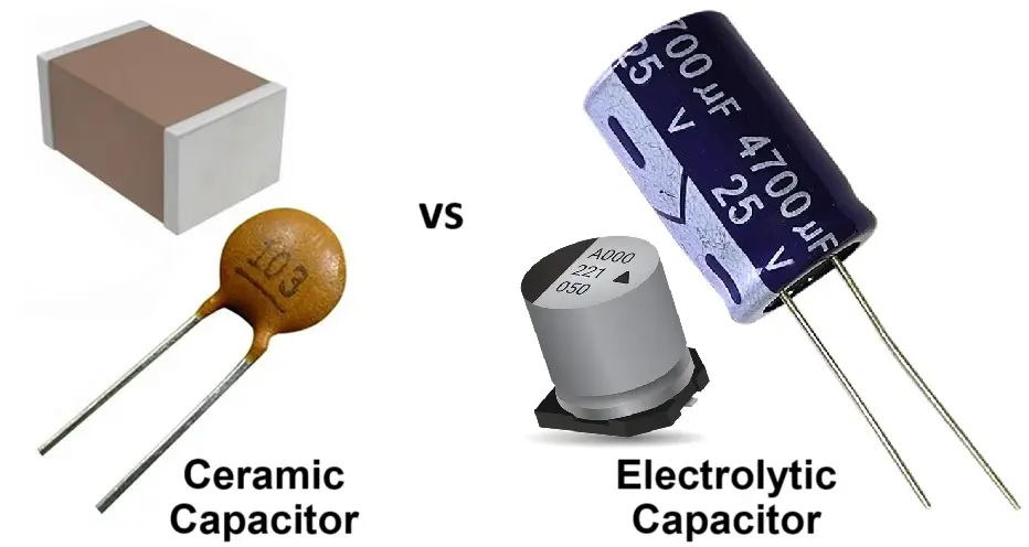
Components like electrolytic capacitors and precision resistors are sensitive to high temperatures, which can degrade their performance or shorten their lifespan. For example, electrolytic capacitors often have a maximum operating temperature of 85°C to 105°C. Placing them near a hot component like a power IC can push them beyond safe limits. Instead, position these sensitive parts in cooler areas of the board, away from major heat sources.
3. Use Copper Planes for Heat Spreading
Copper planes or pours act as thermal conductors, spreading heat across a larger area of the PCB. Connect high-heat components to large copper areas on the board to help dissipate heat more evenly. For multilayer boards, dedicate inner layers to ground or power planes to enhance thermal distribution. A copper plane with a thickness of 1 oz/ft2 can significantly reduce thermal resistance, helping to keep temperatures under control.
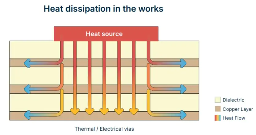
Thermal Vias Placement: Enhancing Heat Transfer
Thermal vias are small, plated-through holes that transfer heat from one side of the PCB to the other, or to inner copper layers. Proper thermal vias placement is crucial for managing heat in multilayer designs or when components are mounted on one side of the board.
1. Place Thermal Vias Under or Near Hot Components
Position thermal vias directly under or adjacent to high-heat components to create a direct path for heat to escape to the opposite side of the board or to a heat sink. For example, under a surface-mount power IC, a grid of 5x5 vias with a diameter of 0.3mm each can significantly reduce thermal resistance.
2. Connect Vias to Copper Planes
For maximum effectiveness, connect thermal vias to large copper planes on both the top and bottom layers of the PCB. This connection allows heat to spread across a wider area, preventing localized overheating. Ensure that vias are filled or plugged if necessary to avoid solder wicking during assembly, which can compromise thermal performance.
3. Optimize Via Density and Size
More vias generally mean better heat transfer, but there’s a balance to strike. Too many vias can weaken the board’s structural integrity or interfere with signal routing. A common guideline is to use vias with a spacing of 1.2mm to 1.5mm in a grid pattern under hot components. Adjust the via diameter and count based on the component’s power dissipation and the board’s thermal requirements.

Heat Sink Placement Guide: Maximizing Cooling Efficiency
Heat sinks are passive cooling devices that absorb and dissipate heat from components into the surrounding air. Proper heat sink placement is essential to ensure they work effectively as part of your PCB temperature control strategy.
1. Attach Heat Sinks to High-Heat Components
Directly mount heat sinks to components with the highest power dissipation, such as voltage regulators or power transistors. Ensure good thermal contact using thermal interface materials (TIMs) like thermal paste or pads, which can reduce thermal resistance to as low as 0.5°C/W depending on the material used.
2. Consider Airflow Direction for Heat Sink Orientation
Align the fins of the heat sink with the direction of airflow in the enclosure. For natural convection, vertical fins work best as they allow hot air to rise. For forced convection with a fan, orient the fins to match the airflow path for maximum heat dissipation. A poorly oriented heat sink can reduce cooling efficiency by up to 30%.
3. Ensure Adequate Clearance Around Heat Sinks
Provide enough space around the heat sink to allow air to circulate freely. Crowding components or placing walls too close to the heat sink can trap heat, reducing its effectiveness. As a rule of thumb, maintain at least 10-15mm of clearance on all sides of the heat sink for optimal performance.

Advanced PCB Temperature Control Techniques
Beyond component placement, thermal vias, and heat sinks, there are additional methods to enhance PCB temperature control, especially for high-performance or high-density designs.
1. Use High-Thermal-Conductivity Materials
Standard FR-4 PCB material has a thermal conductivity of about 0.25 W/m·K, which is relatively low. For better heat dissipation, consider using materials with higher thermal conductivity, such as metal-core PCBs (MCPCBs), which can achieve thermal conductivities of 1-4 W/m·K. These materials are ideal for applications like LED lighting or power electronics.
2. Incorporate Active Cooling Solutions
In cases where passive cooling isn’t enough, active solutions like fans or Peltier coolers can be used. Fans provide forced convection, significantly lowering temperatures in dense designs. For instance, a small 40mm fan can reduce component temperatures by 20-30°C under heavy load, depending on the setup.
3. Simulate Thermal Performance During Design
Use thermal simulation tools during the design phase to predict hot spots and evaluate the effectiveness of your thermal management strategies. Software can model heat flow and temperature distribution, allowing you to adjust component placement and cooling solutions before manufacturing. This step can save significant time and cost by identifying potential issues early.

Common Mistakes to Avoid in Thermal-Aware Design
Even with the best intentions, it’s easy to make mistakes that undermine PCB thermal management. Here are some pitfalls to watch out for:
- Ignoring Component Spacing: Placing components too close together restricts airflow and traps heat. Always adhere to minimum spacing guidelines, especially around high-power parts.
- Overlooking Enclosure Design: A well-designed PCB can still overheat if the enclosure lacks proper ventilation. Ensure the enclosure complements your thermal strategy with vents or fans as needed.
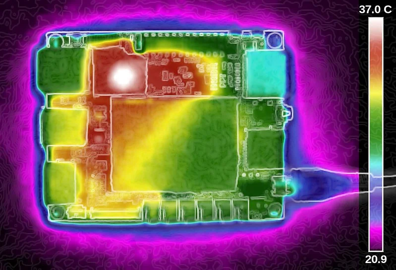
- Neglecting Thermal Testing: Don’t assume your design will work perfectly without testing. Use thermal imaging or temperature probes to verify that components stay within safe limits under real-world conditions.
Conclusion: Building Cooler, More Reliable PCBs
Thermal-aware component placement is a critical aspect of PCB design that directly impacts the performance and reliability of electronic devices. By strategically positioning components for heat dissipation, optimizing thermal vias placement, following a heat sink placement guide, and implementing advanced PCB temperature control techniques, you can prevent overheating and ensure your designs operate safely and efficiently. Remember to spread out heat sources, leverage copper planes, and simulate thermal performance to catch issues early. With these strategies, you’ll be well-equipped to create PCBs that stay cool under any load, delivering long-lasting value to your projects.
Implementing these practices doesn’t just protect your components—it also enhances the overall quality of your designs, making them more reliable for end users. Start applying these thermal management tips in your next project to see the difference a cooler PCB can make.