 ALLPCB


Wave soldering is a critical process in printed circuit board (PCB) assembly, especially for through-hole technology (THT) components. A well-designed wave soldering fixture is essential to ensure precision, protect sensitive areas of the PCB, and improve manufacturing efficiency. If you're looking to optimize your PCB assembly process, understanding the nuances of wave soldering fixture design is key. This guide dives deep into everything you need to know about PCB wave soldering fixture materials, design rules, thermal considerations, cost factors, and manufacturing techniques.
In the following sections, we'll explore each aspect in detail, providing actionable insights for engineers and manufacturers aiming to enhance their wave soldering processes. Whether you're new to PCB assembly or a seasoned professional, this comprehensive resource will help you design fixtures that deliver consistent, high-quality results.
What Is a Wave Soldering Fixture and Why Does It Matter?
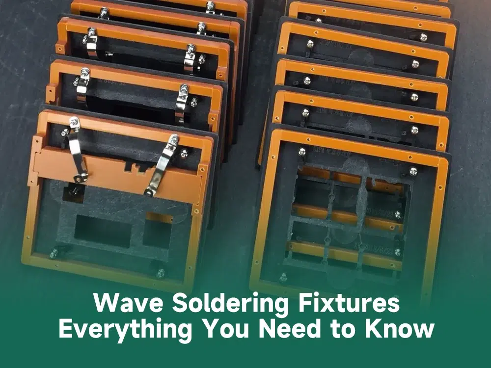
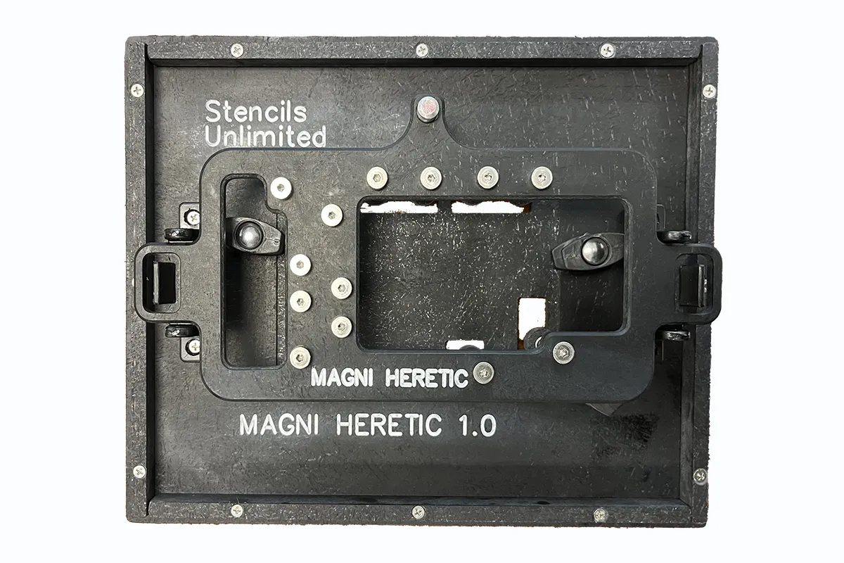
A wave soldering fixture, often called a wave solder pallet, is a custom tool used during the wave soldering process to hold and protect a PCB. It ensures that only specific areas of the board are exposed to the molten solder wave, while shielding sensitive components or regions that don't require soldering. These fixtures are vital for mixed-technology boards where surface-mount devices (SMDs) and THT components coexist, as they prevent damage to pre-soldered parts.
The importance of a well-designed fixture cannot be overstated. A poorly designed fixture can lead to uneven soldering, thermal stress on the PCB, or even component damage, resulting in costly rework or product failures. By focusing on proper design and material selection, you can achieve higher yields, reduce defects, and streamline production.
Key Elements of PCB Wave Soldering Fixture Design Rules
Designing a wave soldering fixture requires careful attention to several rules and guidelines to ensure compatibility with the PCB layout and soldering equipment. Here are the core principles to follow for effective fixture design:
- Component Clearance: Ensure the fixture provides adequate clearance around components to avoid interference during soldering. For instance, taller components like electrolytic capacitors may need deeper cavities in the fixture to prevent contact with the solder wave. A general rule of thumb is to maintain a clearance of at least 2-3 mm around critical parts.
- Board Alignment: The fixture must securely hold the PCB in place to prevent misalignment during the soldering process. Incorporate alignment pins or edges that match the PCB's mounting holes or reference points, ensuring precision within 0.1 mm for high-density boards.
- Solder Wave Access: Design the fixture to expose only the areas of the PCB that require soldering. Use precise cutouts or openings to allow the solder wave to contact through-hole leads while masking off areas with SMDs or pre-soldered components.
- Fixture Stability: The fixture must remain stable on the conveyor system of the wave soldering machine. A flat base and balanced weight distribution are crucial to prevent tipping or vibration during operation.
- Durability for Repeated Use: Since fixtures are reused across multiple soldering cycles, they should withstand mechanical stress and resist warping. This is closely tied to material selection, which we'll discuss in the next section.
By adhering to these design rules, you can create fixtures that enhance the accuracy and repeatability of the wave soldering process, ultimately reducing defects and improving production efficiency.
PCB Wave Soldering Fixture Materials: Choosing the Right One
The material used for a wave soldering fixture plays a significant role in its performance, durability, and cost. The ideal material must withstand high temperatures, resist chemical degradation from flux and solder, and maintain dimensional stability. Here are the most common materials used for PCB wave soldering fixtures:
- ESD-Safe Composite Materials: These materials, often based on fiberglass or synthetic resins, are popular for their excellent thermal resistance and electrostatic discharge (ESD) protection. They can endure temperatures up to 300°C, making them suitable for most wave soldering processes.
- High-Temperature Plastics: Certain engineered plastics are designed to handle the heat of wave soldering (typically 250-260°C for lead-free solder). They are lightweight and cost-effective but may have a shorter lifespan compared to composites.
- Aluminum: For applications requiring high durability, aluminum fixtures are sometimes used. However, they conduct heat rapidly, which can lead to thermal issues if not designed with insulation in mind. Aluminum fixtures are often coated to prevent solder adhesion.
- Ceramic Materials: In rare cases, ceramics are used for fixtures in extremely high-temperature or specialized applications. They offer superior heat resistance but are expensive and brittle.
When selecting a material, consider the specific requirements of your PCB assembly process, such as the type of solder (lead-based or lead-free), the number of soldering cycles, and budget constraints. For most standard applications, ESD-safe composites strike a balance between performance and cost.
PCB Wave Soldering Fixture Thermal Considerations
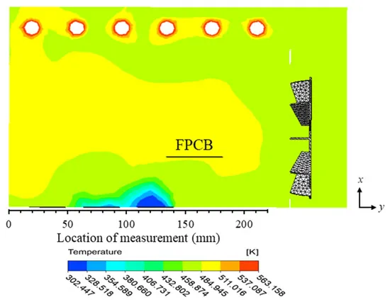
Thermal management is a critical aspect of wave soldering fixture design. The fixture is exposed to high temperatures during the soldering process, and improper heat distribution can damage the PCB or components. Here are key thermal considerations to keep in mind:
- Heat Resistance: The fixture material must resist deformation or degradation at soldering temperatures, which can range from 240°C to 260°C for lead-free solder alloys. Always check the material's maximum operating temperature before use.
- Thermal Conductivity: Materials with high thermal conductivity, like aluminum, can transfer heat to unintended areas of the PCB, causing thermal stress or component damage. If using such materials, incorporate insulating layers or coatings to minimize heat transfer.
- Heat Dissipation: The fixture should help dissipate heat evenly to prevent hotspots on the PCB. Designs with ventilation holes or channels can improve airflow and cooling during and after soldering.
- Preheating Compatibility: Wave soldering often involves a preheating stage to prepare the PCB. Ensure the fixture can handle gradual temperature increases (typically 2-3°C per second) without warping or cracking.
By addressing these thermal factors, you can protect both the fixture and the PCB from damage, ensuring consistent soldering quality over multiple production runs.
PCB Wave Soldering Fixture Cost: Balancing Quality and Budget
The cost of a wave soldering fixture depends on several factors, including material choice, design complexity, and manufacturing method. Here's a breakdown of what influences the cost and how to optimize it without compromising quality:
- Material Costs: High-end materials like ESD-safe composites or ceramics are more expensive than basic plastics. For small to medium production runs, a mid-range material often provides the best value. For example, a composite fixture might cost between $100 and $500, depending on size and customization.
- Design Complexity: Fixtures with intricate cutouts, multiple cavities, or custom alignment features require more design and machining time, increasing costs. Simplifying the design where possible can reduce expenses without affecting performance.
- Volume of Production: If you need fixtures for high-volume manufacturing, consider investing in durable materials that last longer, even if the upfront cost is higher. For low-volume runs, cheaper materials may suffice.
- Reusability: A well-designed fixture can be reused for thousands of soldering cycles, spreading the cost over time. Factor in the fixture's lifespan when evaluating its price.
On average, a custom wave soldering fixture can range from $100 to $1,000 or more, depending on the specifications. To keep costs down, work with your manufacturing partner to optimize the design for both functionality and affordability.
PCB Wave Soldering Fixture Manufacturing: Process and Best Practices
Manufacturing a wave soldering fixture involves precision engineering to ensure it meets the design specifications. Here's an overview of the manufacturing process and tips to achieve the best results:
- CAD Design: Start with a detailed computer-aided design (CAD) model of the fixture, incorporating all necessary features like cutouts, alignment pins, and cavities. Use the PCB's Gerber files or layout data to ensure accuracy.
- CNC Machining: Most fixtures are manufactured using computer numerical control (CNC) machining, which offers high precision for cutting and shaping materials. For complex designs, tolerances as tight as 0.05 mm may be required.
- Material Preparation: Select and prepare the chosen material, ensuring it is free from defects or contaminants that could affect performance during soldering.
- Finishing and Coating: Apply surface treatments or coatings to prevent solder adhesion and enhance durability. For example, some fixtures are coated with a non-stick layer to simplify cleaning after soldering.
- Testing and Validation: Before full-scale production, test the fixture with a sample PCB to verify fit, alignment, and thermal performance. Make adjustments if necessary to avoid issues during mass production.
Partnering with an experienced manufacturer can streamline the fixture production process and ensure high-quality results. Always provide detailed specifications and collaborate closely during the design and testing phases.
Common Challenges in Wave Soldering Fixture Design and How to Overcome Them
Even with careful planning, challenges can arise during the design and use of wave soldering fixtures. Here are some common issues and solutions:
- Solder Bridging: This occurs when excess solder connects adjacent pins or pads. To prevent it, ensure precise cutouts in the fixture and optimize the wave soldering machine's settings for solder flow and temperature.
- Thermal Warping: Fixtures or PCBs may warp due to uneven heat exposure. Use materials with low thermal expansion coefficients and design the fixture with uniform thickness to distribute heat evenly.
- Fixture Wear: Over time, fixtures can degrade from repeated exposure to heat and chemicals. Regularly inspect fixtures for signs of wear and replace them when necessary to maintain soldering quality.
- Misalignment: If the PCB shifts during soldering, it can lead to poor solder joints. Incorporate robust alignment features and double-check the fixture's compatibility with the conveyor system.
By anticipating these challenges and implementing the suggested solutions, you can minimize disruptions and maintain a smooth wave soldering process.
Conclusion: Mastering Wave Soldering Fixture Design for Optimal PCB Assembly
Wave soldering fixtures are indispensable tools for achieving high-quality PCB assembly, especially for boards with through-hole components. By focusing on key aspects like PCB wave soldering fixture materials, design rules, thermal considerations, cost management, and manufacturing techniques, you can create fixtures that enhance efficiency and reduce defects in your production line.
Remember that every PCB project is unique, so tailor your fixture design to the specific requirements of your board layout and soldering process. Whether you're dealing with high-volume manufacturing or a small batch of prototypes, investing time and resources into fixture design will pay off in the form of consistent, reliable results.
With this ultimate guide, you now have the knowledge to tackle wave soldering fixture design with confidence. Apply these principles to your next project, and watch your PCB assembly process reach new levels of precision and productivity.


