ALLPCB


If you're diving into PCB design, you might be wondering how to master silkscreen annotation for clarity and precision. Silkscreen annotation, also known as the silkscreen layer, is the printed text and symbols on a printed circuit board (PCB) that guide assembly, testing, and troubleshooting. In this comprehensive guide, we’ll walk you through everything you need to know about the PCB design silkscreen layer, from a silkscreen annotation tutorial to creating silkscreen markings, choosing silkscreen fonts for PCB, and adopting the best PCB silkscreen practices. Whether you're a beginner or a seasoned designer, this post will help you create effective and professional silkscreen layers for your projects.
What Is Silkscreen Annotation in PCB Design?
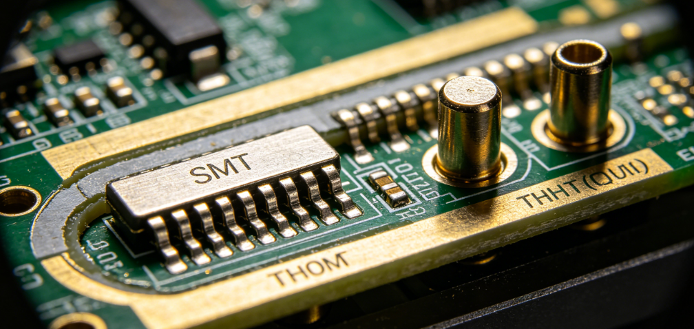
Silkscreen annotation refers to the layer of non-conductive ink applied to the surface of a PCB. This layer includes text, symbols, and markings that provide essential information for manufacturing, assembly, and maintenance. Typically applied on the top or bottom side of the board, the silkscreen layer helps identify components, indicate polarity, and label test points, making it a critical part of the PCB design process.
The silkscreen isn’t just for aesthetics—it plays a functional role. During assembly, it guides technicians on where to place components, and during troubleshooting, it helps engineers quickly locate specific parts or connections. Without a well-designed silkscreen layer, errors can occur, leading to costly rework or delays.

Why Is Silkscreen Annotation Important?
Silkscreen annotation is vital for several reasons in PCB design:
- Component Identification: It labels components like resistors, capacitors, and ICs with reference designators (e.g., R1, C2) so assemblers know exactly what goes where.
- Polarity and Orientation: Markings indicate the correct orientation for polarized components like diodes and electrolytic capacitors, preventing assembly errors.
- Testing and Debugging: Silkscreen labels for test points and connectors make it easier to probe and diagnose issues during testing.
- Manufacturing Efficiency: Clear silkscreen markings reduce the chances of mistakes during automated or manual assembly, saving time and costs.
In short, a well-executed silkscreen layer ensures your PCB is user-friendly and error-free, which is essential for both small-scale prototypes and large production runs.
Key Elements of a PCB Design Silkscreen Layer
Before diving into a silkscreen annotation tutorial, let’s break down the core elements that should be included in your silkscreen layer:
- Reference Designators: These are alphanumeric codes (e.g., R1 for a resistor, U1 for an IC) that match the schematic and help identify each component on the board.
- Polarity Indicators: Symbols like a "+" or "-" for capacitors or a small dot for diode anodes ensure components are placed correctly.
- Pin Numbers: For ICs or connectors, labeling pin 1 or other key pins helps with orientation during assembly.
- Board Information: Include details like the board name, version number, or date to track revisions and ensure the right design is used.
- Warnings or Instructions: Markings like "High Voltage" or "Do Not Touch" can alert users to potential hazards.
Each of these elements must be placed strategically to avoid clutter and ensure readability, which we’ll cover in the best PCB silkscreen practices section.
Silkscreen Annotation Tutorial: Step-by-Step Guide
Creating an effective silkscreen layer doesn’t have to be complicated. Follow these steps to design a clear and functional silkscreen for your PCB:
Step 1: Plan Your Silkscreen Layout
Before adding any text or symbols, review your PCB layout to identify where components, traces, and vias are located. Ensure that silkscreen markings won’t overlap with solder pads or areas where components will be mounted. Keep markings close to the relevant components but leave enough space to avoid confusion.
Step 2: Use Reference Designators
Assign reference designators to each component based on your schematic. Place these labels next to the corresponding component footprints. For example, if you have a resistor labeled R1 in your schematic, ensure "R1" is printed near the resistor’s footprint on the PCB.
Step 3: Add Polarity and Orientation Markings
For components like diodes, capacitors, and ICs, include polarity or orientation indicators. A small dot or line near pin 1 of an IC or a "+" symbol near the positive terminal of a capacitor can prevent assembly errors.
Step 4: Choose the Right Font and Size
When creating silkscreen markings, readability is key. Use a simple, sans-serif font with a minimum height of 0.8 mm (31 mils) to ensure legibility. Avoid overly decorative fonts that might be hard to read after printing. Common font sizes range from 0.8 mm to 1.5 mm (31 to 59 mils), depending on the board size and available space.
Step 5: Position Markings Consistently
Maintain a uniform reading direction for all text—preferably left to right and top to bottom. Avoid rotating text unless absolutely necessary, as inconsistent orientations can confuse assemblers.
Step 6: Include Board Information
Add essential details like the board name, revision number, or manufacturing date in a corner of the PCB. This helps with version control and traceability during production.
Step 7: Review and Test
Before finalizing your design, double-check the silkscreen layer for errors or overlaps. Many PCB design tools allow you to preview the silkscreen layer in 3D to ensure everything is legible and correctly placed. If possible, print a 1:1 scale paper mockup to verify readability.

Creating Silkscreen Markings: Tips for Precision
When creating silkscreen markings, precision and clarity are essential to avoid misinterpretation. Here are some practical tips to ensure your markings are effective:
- Avoid Overcrowding: Only include necessary information. Too many markings can clutter the board and make it hard to read. Prioritize reference designators and polarity indicators over optional labels.
- Use Clear Symbols: For polarity, use universally recognized symbols like a "+" or a small arrow. Avoid custom symbols that might confuse assemblers unfamiliar with your design.
- Maintain Clearance: Keep silkscreen markings at least 0.2 mm (8 mils) away from solder pads and vias to prevent ink from interfering with soldering processes.
- Color Contrast: Most silkscreen ink is white on dark boards or black on light boards. Ensure there’s enough contrast between the ink and the board’s solder mask for visibility.
By focusing on these details, you can create silkscreen markings that are both functional and professional.
Silkscreen Fonts for PCB: Choosing the Right One
Selecting the appropriate silkscreen fonts for PCB design is crucial for readability and manufacturability. Not all fonts are suitable for silkscreen printing due to limitations in resolution and ink application. Here’s what to consider when choosing fonts:
- Stick to Simple Fonts: Use sans-serif fonts like Arial or Helvetica, as they are clean and easy to read even at small sizes. Avoid serif fonts or scripts with fine details that may not print clearly.
- Minimum Size: As mentioned earlier, text should be at least 0.8 mm (31 mils) tall with a stroke width of 0.15 mm (6 mils) to ensure it’s legible after printing.
- Consistency: Use the same font and size across the entire board for a uniform look. Mixing fonts can make the silkscreen appear unprofessional.
- Software Compatibility: Ensure the font you choose is supported by your PCB design software and the manufacturer’s printing process. Some custom fonts may not translate well during fabrication.
Following these guidelines will help ensure your silkscreen fonts for PCB are clear and effective, reducing the risk of errors during assembly.
Best PCB Silkscreen Practices for Optimal Results
To elevate your PCB design, adopting the best PCB silkscreen practices is essential. These practices, gathered from industry standards and expert recommendations, will help you create a silkscreen layer that enhances both functionality and manufacturability:
1. Follow Industry Standards
Adhere to guidelines like those from the Institute of Printed Circuits (IPC), such as IPC-7351 for component footprints and silkscreen placement. These standards ensure your design meets common manufacturing and assembly expectations.
2. Prioritize Readability Over Aesthetics
While it might be tempting to get creative with your silkscreen, always prioritize readability. Avoid placing text too close to edges or over areas that might be covered by components after assembly.
3. Use Minimal Text for Dense Boards
For densely populated PCBs, limit silkscreen text to critical information only, such as reference designators and polarity markers. If space is tight, consider placing additional details in assembly documentation rather than on the board.
4. Account for Manufacturing Tolerances
Silkscreen printing isn’t always perfectly aligned due to manufacturing tolerances, which can be as much as ±0.1 mm (4 mils). Leave extra clearance around text and symbols to account for potential misalignment.
5. Test with Your Manufacturer
Different manufacturers have varying capabilities for silkscreen resolution and ink application. Send a test design or consult with your fabrication partner to confirm that your silkscreen layer meets their requirements.
6. Avoid Interference with Electrical Properties
Ensure that silkscreen ink doesn’t overlap with areas critical to electrical performance, such as high-frequency traces or impedance-controlled lines. While silkscreen ink is non-conductive, its presence can slightly alter dielectric properties in sensitive areas.

Common Mistakes to Avoid in Silkscreen Annotation
Even experienced designers can make mistakes when creating a silkscreen layer. Here are some common pitfalls to watch out for:
- Placing Text Over Solder Pads: This can cause the text to be unreadable after soldering or interfere with the soldering process itself. Always maintain a clearance of at least 0.2 mm (8 mils).
- Using Unreadable Fonts or Sizes: Text smaller than 0.8 mm (31 mils) or overly complex fonts can become blurred or illegible after printing.
- Inconsistent Orientation: Rotating text in different directions makes it harder to read and can lead to assembly mistakes.
- Ignoring Manufacturer Guidelines: Some manufacturers have specific rules for silkscreen layers, such as maximum text density or restricted areas. Failing to follow these can result in rejected boards.
By being mindful of these issues, you can save time and avoid costly redesigns during the manufacturing process.
Conclusion: Mastering Silkscreen Annotation for Better PCB Design
Silkscreen annotation is a small but critical part of PCB design that can make a big difference in the success of your project. By understanding the purpose of the PCB design silkscreen layer, following a structured silkscreen annotation tutorial, creating clear silkscreen markings, choosing appropriate silkscreen fonts for PCB, and adopting the best PCB silkscreen practices, you can ensure your boards are easy to assemble, test, and maintain.
Take the time to plan your silkscreen layer carefully, prioritize readability, and collaborate with your manufacturer to meet their specifications. With these steps, you’ll be well on your way to creating professional, error-free PCBs that stand out for all the right reasons. Whether you’re working on a simple prototype or a complex multilayer board, a well-designed silkscreen layer is an investment in quality and efficiency.