In the world of electronics, designing a printed circuit board (PCB) for high-speed digital interfaces like USB, HDMI, and Ethernet is a critical task. These interfaces transmit data at incredibly fast rates, and any small error in the PCB layout can lead to signal loss, interference, or complete failure. So, how do you optimize a PCB layout for high-speed interfaces? The key lies in focusing on signal integrity, proper routing techniques, impedance matching, and noise reduction.
In this comprehensive guide, we'll dive deep into the essentials of high-speed PCB layout optimization. Whether you're working on USB PCB design, HDMI PCB design, or Ethernet PCB design, you'll find practical tips and strategies to ensure your board performs reliably. Let’s explore the critical aspects of designing for signal integrity in high-speed applications and provide you with actionable steps to achieve top-notch results.
Why High-Speed PCB Layout Matters
High-speed digital interfaces operate at frequencies where even tiny design flaws can cause major issues. For instance, USB 3.0 can reach speeds up to 5 Gbps, HDMI 2.0 supports up to 18 Gbps, and Ethernet standards like 10GbE push data rates even higher. At these speeds, signals are highly sensitive to factors like trace length mismatches, crosstalk, and electromagnetic interference (EMI).
A poorly designed PCB layout can result in signal degradation, data errors, or even complete system failure. Optimizing your PCB layout for high-speed interfaces ensures that signals travel cleanly from source to destination, maintaining signal integrity and meeting performance standards. Let’s break down the core principles and techniques for achieving this in your designs.
Understanding Signal Integrity in High-Speed PCB Design
Signal integrity refers to the quality of an electrical signal as it travels through a PCB. In high-speed designs, maintaining signal integrity is crucial to prevent issues like signal distortion, timing errors, and noise. Several factors affect signal integrity, including trace impedance, crosstalk, and reflections.
For USB, HDMI, and Ethernet interfaces, signal integrity challenges often arise from high-frequency signals. These signals can behave like waves rather than simple electrical currents, making them prone to interference and loss. By focusing on specific layout techniques, you can minimize these risks and ensure reliable performance.
Key Principles for High-Speed PCB Layout Optimization
1. Impedance Matching for Signal Consistency
Impedance matching is a cornerstone of high-speed PCB design. Each high-speed interface has a specific characteristic impedance that must be maintained across the signal path. For example, USB 2.0 and 3.0 typically require a differential impedance of 90 ohms, HDMI traces often target 100 ohms, and Ethernet designs may vary between 85 to 100 ohms depending on the standard.
To achieve proper impedance, calculate the trace width and spacing based on the PCB stack-up and dielectric material. Use controlled impedance traces and avoid sudden changes in trace width or layer transitions, as these can cause signal reflections. Many design tools offer impedance calculators to help with this process, ensuring your traces meet the required specifications.
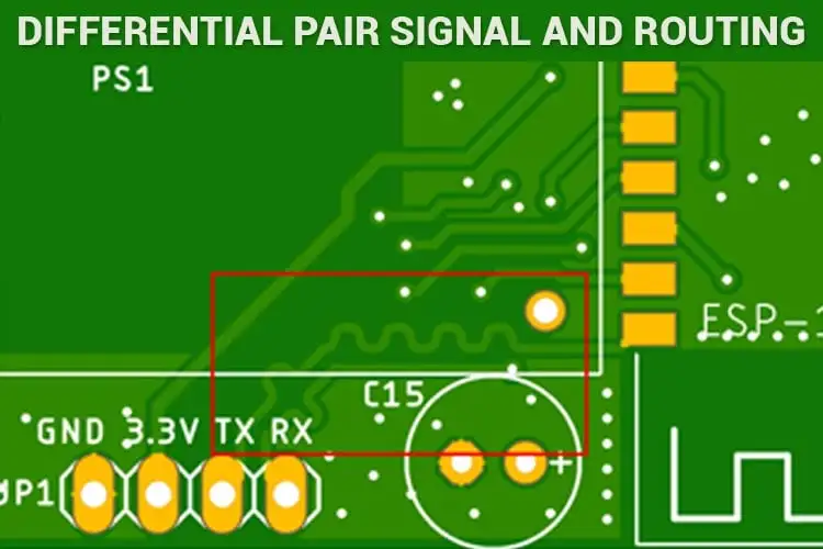
2. Differential Pair Routing for USB and HDMI
High-speed interfaces like USB and HDMI rely on differential signaling, where two traces carry complementary signals to reduce noise. For optimal performance, keep differential pairs tightly coupled by maintaining consistent spacing between the traces. Avoid routing over splits in the ground plane, as this can introduce noise and disrupt signal integrity.
Match the lengths of differential pairs to within a few mils (thousandths of an inch) to prevent timing skew. For USB 3.0, length mismatches should be less than 5 mils, while HDMI may require even tighter tolerances. Use serpentine routing if needed to equalize trace lengths, but minimize sharp bends to avoid signal degradation.
3. Ground Planes and Return Paths
A solid ground plane is essential for high-speed PCB layouts. It provides a low-impedance return path for signals and helps reduce EMI. Avoid splitting the ground plane under high-speed traces, as this forces return currents to take longer paths, leading to noise and signal integrity issues.
For multilayer PCBs, dedicate at least one layer to a continuous ground plane. Place this layer directly beneath the signal layer to minimize loop inductance. For interfaces like Ethernet, which often involve multiple signal pairs, ensure that the ground plane extends under all high-speed traces to maintain a consistent reference.
4. Minimize Crosstalk in Ethernet PCB Design
Crosstalk occurs when signals from one trace interfere with another, a common issue in densely packed Ethernet designs. To reduce crosstalk, increase the spacing between adjacent signal pairs. A general rule of thumb is to keep spacing at least three times the trace width (3W rule) for high-speed signals.
Additionally, route high-speed traces on different layers if possible, using ground planes to isolate them. For Ethernet designs supporting 1GbE or 10GbE, pay special attention to the layout of twisted pair signals to avoid interference between transmit and receive channels.
5. Power Supply Decoupling and Noise Reduction
High-speed interfaces are sensitive to power supply noise, which can degrade signal quality. Place decoupling capacitors close to the power pins of ICs to filter out noise. Use a combination of capacitor values (e.g., 0.1 μF and 1 μF) to cover a wide range of frequencies.
For USB and HDMI designs, ensure that the power delivery network (PDN) has low impedance at high frequencies. This can be achieved by using multiple vias to connect power and ground planes, reducing inductance in the power path.
Specific Considerations for USB, HDMI, and Ethernet PCB Design
USB PCB Design Tips
USB interfaces, especially USB 3.0 and above, demand precise layout techniques due to their high data rates. Route differential pairs with minimal vias, as each via introduces impedance discontinuities. If vias are unavoidable, use back-drilling to remove unused via stubs, which can cause signal reflections.
Keep USB traces as short as possible to reduce signal loss. For USB 3.0, the maximum recommended trace length is around 15 inches, though shorter lengths are ideal. Shielding is also critical—place ground vias along the edges of USB traces to create a Faraday cage effect, reducing EMI.
HDMI PCB Design Challenges
HDMI designs handle extremely high data rates, making them prone to signal integrity issues. The HDMI 2.0 standard, for instance, supports 6 Gbps per channel, requiring strict control over trace lengths and impedance. Length matching for differential pairs should be within 2 mils to avoid skew.
Avoid routing HDMI traces near noisy components like switching regulators. Use a multilayer stack-up with dedicated ground and power planes to isolate signals. If your design includes connectors, ensure that the connector footprint matches the impedance of the traces to prevent mismatches.
Ethernet PCB Design Strategies
Ethernet layouts, particularly for 1GbE and 10GbE, require careful planning to handle multiple high-speed pairs. Use magnetics (transformers) close to the Ethernet connector to filter common-mode noise. Route differential pairs symmetrically and avoid crossing them with other high-speed signals.
For Ethernet designs, maintain a 100-ohm differential impedance for most standards. Test your layout with simulation tools to verify signal integrity, especially for longer trace runs. Shielded connectors and proper grounding at the connector interface can further reduce noise in Ethernet applications.
Tools and Techniques for High-Speed PCB Layout
Designing for high-speed interfaces requires the right tools and methodologies. Modern PCB design software offers features like impedance calculators, signal integrity simulators, and auto-routing for differential pairs. Use these tools to validate your layout before fabrication.
Perform pre-layout simulations to identify potential issues like crosstalk or impedance mismatches. Post-layout analysis, such as time-domain reflectometry (TDR), can help verify that your design meets the required specifications. Additionally, consider working with a manufacturer that offers design rule checks (DRC) tailored for high-speed layouts.
Common Mistakes to Avoid in High-Speed PCB Design
Even experienced designers can make errors in high-speed layouts. Here are some pitfalls to watch out for:
- Ignoring Stack-Up Design: A poorly planned stack-up can lead to impedance issues and noise. Always define your layer stack early in the design process.
- Neglecting Length Matching: Even small mismatches in trace lengths can cause timing errors in USB, HDMI, and Ethernet designs.
- Overusing Vias: Excessive vias disrupt signal paths and introduce parasitic effects. Minimize their use in high-speed traces.
- Poor Grounding: Inadequate ground planes or splits under traces can degrade signal integrity and increase EMI.
Testing and Validation for High-Speed Interfaces
After completing your PCB layout, testing is crucial to ensure performance. Use an oscilloscope to measure eye diagrams, which provide insight into signal quality and timing margins. For USB and HDMI, check for jitter and skew within the specified limits of the standard.
For Ethernet designs, perform bit error rate (BER) testing to confirm data integrity across all channels. If issues are detected, revisit your layout to address impedance mismatches, crosstalk, or noise sources. Iterating on your design based on test data is often necessary to achieve optimal results.
Conclusion: Mastering High-Speed PCB Layout Optimization
Optimizing a PCB layout for high-speed digital interfaces like USB, HDMI, and Ethernet is both a science and an art. By prioritizing signal integrity, impedance matching, and noise reduction, you can create designs that perform reliably even at the highest data rates. Whether you're focusing on USB PCB design, HDMI PCB design, or Ethernet PCB design, the principles of high-speed PCB layout remain the same—plan carefully, simulate often, and test thoroughly.
With the strategies outlined in this guide, you’re equipped to tackle the challenges of high-speed design. From differential pair routing to grounding techniques, every detail matters. Apply these tips to your next project, and you’ll see the difference in performance and reliability. Crafting a high-speed PCB layout may be complex, but the results are well worth the effort.
 ALLPCB


