 ALLPCB


Are you looking to understand the PCB via filling process and how it impacts your printed circuit board designs? Via filling is a critical step in PCB manufacturing that enhances reliability, improves electrical and thermal performance, and ensures the longevity of your boards. In this comprehensive guide, we’ll explore the different types of via filling, compare conductive vs non-conductive via filling, analyze via filling materials, dive into via filling cost analysis, and review IPC standards for via filling. Whether you’re an engineer or a designer, this guide will provide actionable insights to optimize your PCB projects.
What Is PCB Via Filling and Why Does It Matter?
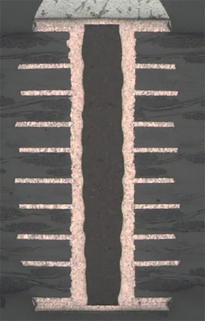
Via filling is a process in PCB manufacturing where the small holes, or vias, that connect different layers of a circuit board are filled with a specific material. These vias are essential for creating electrical connections between layers, but leaving them open can lead to issues like solder wicking, air entrapment, or structural weakness. Filling these vias addresses these problems and improves the overall performance of the board.
The importance of via filling lies in its ability to enhance signal integrity, provide better thermal management, and increase the mechanical strength of the PCB. For high-density interconnect (HDI) boards or designs with strict performance requirements, via filling can be a game-changer. Let’s dive deeper into the specifics of this process and explore its various aspects.
Types of PCB Via Filling
There are several methods used in the PCB via filling process, each with unique characteristics and applications. Understanding these types will help you choose the right one for your design needs.
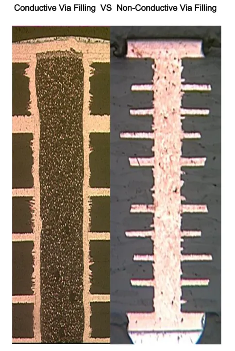
1. Conductive Via Filling
Conductive via filling involves using materials that conduct electricity to fill the via holes. This method is often chosen when you need to maintain or enhance electrical connectivity between layers. Common materials for conductive fills include silver or copper-based epoxy. These materials not only fill the via but also contribute to the electrical performance of the board by reducing resistance.
For example, in high-frequency applications, conductive fills can help maintain signal integrity by minimizing impedance mismatches. A typical conductive fill might reduce via resistance to as low as 1-2 milliohms, depending on the material and via size.
2. Non-Conductive Via Filling
In contrast, non-conductive via filling uses materials like epoxy resin that do not conduct electricity. This type of filling is primarily used to provide structural support and prevent issues like solder migration during assembly. Non-conductive fills are ideal for vias that don’t require an electrical connection through the fill material itself.
Non-conductive fills are often used in designs where isolation between layers is critical. They also help in preventing air bubbles or voids during the soldering process, which can compromise the board’s reliability.
3. Copper-Plated Shut Vias
This method involves completely closing the via with copper plating, creating a solid metal structure. Copper-plated shut vias are highly reliable for both electrical and thermal conductivity. They are often used in advanced designs where thermal dissipation is a priority, as copper can effectively transfer heat away from critical components.
This process, while effective, can be more complex and costly due to the additional plating steps involved. However, for applications requiring robust performance, such as in aerospace or automotive electronics, the benefits often outweigh the costs.
Conductive vs Non-Conductive Via Filling: A Detailed Comparison
When deciding between conductive vs non-conductive via filling, several factors come into play. Let’s break down the key differences to help you make an informed choice for your PCB design.
- Electrical Performance: Conductive fills enhance electrical connectivity and are ideal for high-speed or high-frequency designs where signal integrity is crucial. Non-conductive fills, on the other hand, are better suited for isolation purposes and do not contribute to electrical pathways.
- Thermal Management: Conductive materials like copper or silver epoxy can improve heat dissipation, making them suitable for power-intensive applications. Non-conductive fills have limited thermal conductivity and are less effective in managing heat.
- Structural Integrity: Both types provide structural support, but non-conductive fills are often preferred for preventing solder wicking and maintaining pad stability during assembly.
- Application Suitability: Conductive fills are commonly used in HDI boards and RF designs, while non-conductive fills are more typical in standard multilayer boards where cost and simplicity are priorities.
Choosing between these options depends on your specific design requirements. For instance, a board operating at signal speeds above 5 GHz might benefit more from conductive fills to minimize signal loss, whereas a simpler consumer electronics board might suffice with a non-conductive fill for cost efficiency.
Via Filling Materials Comparison
The choice of material in the via filling materials comparison significantly affects the performance, cost, and manufacturing process of your PCB. Below are the most commonly used materials and their properties.
1. Epoxy Resin (Non-Conductive)
Epoxy resin is a popular choice for non-conductive via filling due to its low cost and ease of application. It provides excellent structural support and prevents issues like solder migration. However, its thermal conductivity is low, typically around 0.2-0.3 W/m·K, making it less suitable for heat dissipation.
2. Silver Epoxy (Conductive)
Silver epoxy is a conductive material known for its high electrical conductivity, often achieving resistivity values as low as 0.001 ohm-cm. It’s ideal for applications requiring minimal signal loss. However, silver epoxy is more expensive and can be challenging to apply uniformly in high-volume production.
3. Copper Epoxy (Conductive)
Copper epoxy offers a balance between cost and performance. It has good electrical conductivity, though not as high as silver, with resistivity typically around 0.005 ohm-cm. It’s often used in designs where cost is a concern, but some level of conductivity is still required.
4. Copper Plating
Copper plating for shut vias provides superior electrical and thermal conductivity, with thermal conductivity values around 400 W/m·K. It’s the go-to choice for high-performance boards but comes with higher manufacturing complexity and cost due to the plating process.
Via Filling Cost Analysis
Understanding the via filling cost analysis is crucial for balancing performance and budget in your PCB projects. Costs can vary based on the type of filling, materials used, and the complexity of the manufacturing process. Here’s a breakdown of the key cost factors.
- Material Costs: Non-conductive epoxy resin is generally the most affordable, often costing less per board compared to conductive materials like silver epoxy, which can be 2-3 times more expensive due to the cost of silver particles. Copper plating for shut vias tends to be the priciest due to the material and process requirements.
- Manufacturing Complexity: Conductive filling and copper plating require more precise application techniques and additional process steps, increasing labor and equipment costs. Non-conductive filling is simpler and faster, reducing overall production expenses.
- Volume and Scale: For high-volume production, the cost per board for conductive fills or copper plating may decrease due to economies of scale. However, for small runs or prototypes, non-conductive fills are often more cost-effective.
- Design Requirements: High-performance designs that require specific impedance control (e.g., maintaining 50 ohms for RF signals) or enhanced thermal management will naturally incur higher costs due to the need for premium materials and processes.
As a general estimate, non-conductive via filling might add only a small percentage to the total PCB cost, while conductive filling or copper plating could increase costs by 10-20% or more, depending on the board’s specifications. Always weigh these costs against the performance benefits for your specific application.
IPC Standards for Via Filling
Adhering to IPC standards for via filling ensures that your PCB meets industry benchmarks for quality and reliability. The Institute of Printed Circuits (IPC) provides guidelines that cover various aspects of PCB design and manufacturing, including via filling. Here are the key standards to consider.
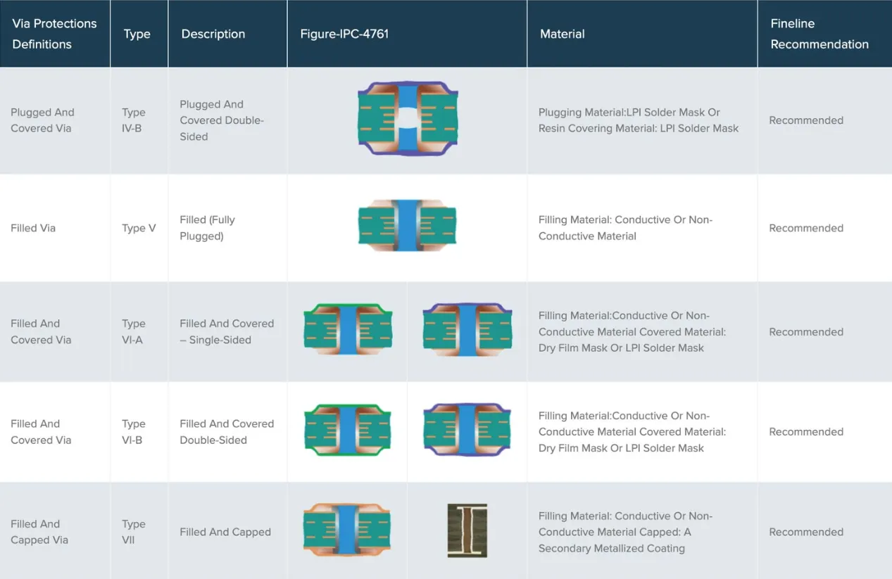
IPC-4761: Design Guide for Protection of Printed Board Via Structures
This standard outlines different types of via protection, including tenting, plugging, and filling. It categorizes via filling into conductive and non-conductive types and provides detailed specifications for each. For instance, it specifies acceptable fill percentages (often 75-100% fill for reliability) and acceptable void levels within filled vias.
IPC-6012: Qualification and Performance Specification for Rigid Printed Boards
IPC-6012 sets performance criteria for rigid PCBs, including requirements for via filling in Class 2 and Class 3 boards. Class 3 boards, used in high-reliability applications like medical or aerospace, have stricter requirements for fill quality and material properties to ensure long-term performance under harsh conditions.
IPC-A-610: Acceptability of Electronic Assemblies
This standard focuses on the final assembly and includes criteria for inspecting filled vias. It ensures that the filling process does not introduce defects like voids or incomplete fills that could affect solderability or reliability.
Following these standards is essential for producing PCBs that meet customer expectations and perform reliably in real-world applications. Ensure that your manufacturing partner is familiar with these guidelines to avoid costly rework or failures.
Manufacturing Process for PCB Via Filling
The PCB via filling process involves several steps to ensure that vias are filled correctly and meet design specifications. While the exact process may vary depending on the type of fill and material, here’s a general overview of how it’s done.
- Via Drilling: The process begins with drilling vias into the PCB to create pathways between layers. These holes must be clean and free of debris to ensure proper filling.
- Plating (if applicable): For conductive vias or copper-plated shut vias, a thin layer of copper is often plated onto the via walls to establish electrical connectivity before filling.
- Filling: The chosen material (epoxy, conductive paste, etc.) is applied to fill the vias. This can be done using screen printing, vacuum filling, or other techniques to ensure uniform distribution and minimal voids.
- Curing: After filling, the material is cured, often through heat or UV exposure, to harden and stabilize it within the via.
- Planarization: Excess material is removed from the surface of the board to create a flat, smooth finish, ensuring that the filled vias do not interfere with subsequent layers or components.
- Inspection: Finally, the filled vias are inspected for quality, checking for issues like incomplete fills or voids using X-ray or visual inspection methods.
Each step requires precision to avoid defects that could compromise the board’s performance. Working with an experienced manufacturer can help ensure that the process is executed flawlessly.
Benefits of Via Filling in PCB Design
Via filling offers several advantages that make it a valuable process in PCB manufacturing. Here are some of the key benefits.
- Improved Reliability: Filled vias prevent issues like solder wicking and air entrapment, reducing the risk of failures during assembly or operation.
- Better Signal Integrity: Conductive fills help maintain consistent impedance, crucial for high-speed designs where signal loss can be a problem.
- Enhanced Thermal Performance: Materials like copper improve heat dissipation, protecting components from overheating in power-intensive applications.
- Support for HDI Designs: Via filling enables the use of via-in-pad technology, allowing for smaller, denser boards without sacrificing reliability.
Choosing the Right Via Filling for Your PCB
Selecting the appropriate via filling method depends on several factors, including your design requirements, budget, and performance goals. Consider the following when making your decision.
- Application Needs: High-frequency or high-power designs may require conductive fills or copper plating for optimal performance.
- Budget Constraints: If cost is a primary concern, non-conductive epoxy fills offer a reliable yet affordable solution.
- Manufacturing Capabilities: Ensure that your manufacturing partner has the expertise and equipment to handle the chosen filling method.
By carefully evaluating these factors, you can choose a via filling approach that balances performance and cost for your specific project.
Conclusion
Via filling is a vital aspect of PCB manufacturing that can significantly impact the performance, reliability, and cost of your circuit boards. Whether you’re comparing conductive vs non-conductive via filling, analyzing via filling materials, or considering via filling cost, understanding the nuances of the PCB via filling process is essential for making informed design decisions. Additionally, adhering to IPC standards for via filling ensures that your boards meet industry benchmarks for quality and durability.
At ALLPCB, we’re committed to helping you navigate these choices with expert guidance and high-quality manufacturing services. By leveraging the insights from this guide, you can optimize your PCB designs for success in any application. Explore our resources and services to take your projects to the next level.


