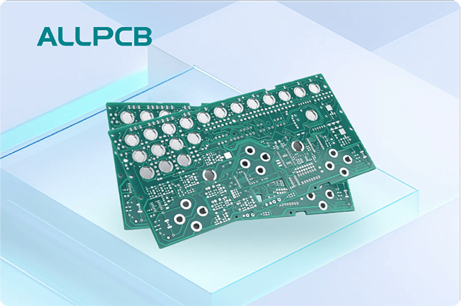
If you're looking for a comprehensive DFT checklist to ensure testability in your PCB designs, you've come to the right place. Design for Testability (DFT) is a critical step in the PCB design process that helps identify issues like shorts, open circuits, and faulty components before production. By following a structured approach with clear guidelines and best practices, you can save time, reduce costs, and improve the reliability of your boards. In this blog, we’ll walk you through a detailed DFT checklist, share essential guidelines, and provide actionable tips for DFT review and sign-off.
Let’s dive into the world of DFT and explore how to make your PCB designs not only functional but also easy to test and manufacture. Whether you're a beginner or an experienced engineer, this guide will help you streamline your design process and avoid common pitfalls.
What is Design for Testability (DFT) in PCB Design?
Design for Testability, or DFT, is a design approach that focuses on making printed circuit boards (PCBs) easier to test during manufacturing and assembly. The goal of DFT is to ensure that potential issues—such as incorrect component placement, soldering defects, or circuit failures—can be detected and resolved early in the process. Studies show that testing costs can account for up to 25-30% of the total production cost of a PCB, so optimizing for testability can lead to significant savings.
DFT involves adding specific features to your design, like test points and accessible pin locations, to simplify testing methods such as In-Circuit Testing (ICT) and Automated Optical Inspection (AOI). By incorporating DFT principles early in the schematic phase, you can avoid costly redesigns and ensure a smoother transition from prototype to production.
Why is DFT Important for PCB Designs?
Without proper DFT, testing a PCB can become a time-consuming and expensive process. Poor testability might result in undetected defects, leading to product failures after assembly or even in the field. Here are a few reasons why DFT is crucial:
- Cost Reduction: Early detection of faults reduces rework and scrap rates.
- Improved Quality: Ensures that boards meet performance and reliability standards.
- Faster Time-to-Market: Streamlined testing processes speed up production cycles.
The Ultimate DFT Checklist for PCB Designs
To help you achieve optimal testability, we’ve compiled a detailed DFT checklist. This list covers key areas to focus on during the design phase, ensuring that your PCB is ready for efficient testing. Use this as a guide for DFT review and sign-off before sending your design to manufacturing.
1. Define Test Requirements Early
Start by identifying the testing needs of your PCB during the schematic design phase. Determine which nets or components are most critical and likely to fail. For example, high-speed signal lines with impedance requirements (e.g., 50 ohms for USB or Ethernet signals) often need specific test points to verify signal integrity at speeds up to 5 Gbps or more.
- Decide on the type of tests, such as ICT, AOI, or functional testing.
- Identify critical nets that require 100% test coverage.
- Document test requirements for collaboration with manufacturing teams.
2. Add Accessible Test Points
Test points are essential for probing during testing. They allow test equipment to access specific nets without damaging the board. Follow these guidelines for placement:
- Place test points on all critical nets, especially power, ground, and high-speed signals.
- Ensure test points are at least 2 mm apart to avoid interference during probing.
- Position test points on the bottom side of the board for easier access during ICT.
3. Optimize Component Placement for Testing
Component placement directly impacts how easily a board can be tested. Crowded designs or poorly placed components can block access to test points or make automated testing impossible.
- Avoid placing components too close to test points (maintain a clearance of at least 1.5 mm).
- Group components logically to simplify visual inspection and probing.
- Ensure tall components don’t obstruct test fixtures or optical inspection cameras.
4. Design for In-Circuit Testing (ICT)
ICT is a common method for checking component placement and soldering quality. To support ICT, your design must accommodate test fixtures and probes.
- Provide test pads with a minimum diameter of 1 mm for probe contact.
- Ensure test pads are free of solder mask for reliable connections.
- Align test points in a grid pattern if possible, as this matches standard ICT fixtures.
5. Support Automated Optical Inspection (AOI)
AOI uses cameras to inspect PCBs for defects like missing components or poor soldering. To make your board AOI-friendly:
- Use clear silkscreen markings for component identification.
- Avoid reflective surfaces near critical areas, as they can interfere with camera accuracy.
- Ensure component polarity markings are visible and consistent.
6. Plan for Functional Testing
Functional testing verifies that the PCB performs as intended under real-world conditions. Incorporate features in your design to support this:
- Add connectors or headers for external test equipment.
- Include diagnostic LEDs or status indicators for quick visual feedback.
- Design with debug interfaces (e.g., JTAG) for firmware and hardware testing.
7. Minimize Signal Interference During Testing
High-speed or sensitive circuits can be affected by test probes or equipment, leading to false results. Protect signal integrity with these practices:
- Route critical signals away from test points to avoid noise pickup.
- Use ground planes to shield sensitive areas from interference.
- Keep test point traces short (less than 10 mm) to minimize parasitic effects.
8. Document Test Specifications
Clear documentation is vital for ensuring that manufacturing and testing teams understand your DFT intent. Include the following in your design files:
- A test point map showing the location and purpose of each test point.
- Specifications for test equipment compatibility (e.g., probe sizes or fixture types).
- Expected test results for critical nets, such as voltage levels or signal timing.
9. Review DFT Compliance Before Sign-Off
Before finalizing your design, conduct a thorough DFT review to catch any overlooked issues. Use this mini-checklist for sign-off:
- Are all critical nets accessible for testing?
- Do test points meet spacing and size requirements?
- Is the design compatible with planned testing methods (ICT, AOI, etc.)?
- Have potential interference issues been addressed?
DFT Guidelines and Best Practices
Beyond the checklist, following established DFT guidelines and best practices can elevate the quality of your PCB designs. Here are some proven strategies to keep in mind during the design process.
Start DFT in the Schematic Phase
One of the most effective DFT best practices is to incorporate testability features during the schematic design, not as an afterthought during layout. Identify critical nets early and plan test point locations before routing begins. This proactive approach prevents the need for major revisions later.
Collaborate with Manufacturing Teams
Work closely with your manufacturing and assembly partners to understand their testing capabilities and limitations. For instance, if they use a specific ICT fixture, ensure your test points align with their probe grid. Collaboration can also help you avoid design choices that increase testing costs or complexity.
Prioritize Test Coverage
Aim for at least 90-95% test coverage on critical nets, especially for power, ground, and high-speed signals. While 100% coverage may not always be feasible due to space constraints, focusing on high-risk areas ensures that major issues are caught during testing.
Keep Future Revisions in Mind
Design with scalability and future updates in mind. If your PCB might need modifications, ensure that test points and debug interfaces remain accessible even after changes. This foresight can save significant time during debugging or redesigns.
Common DFT Mistakes to Avoid
Even with a solid checklist, it’s easy to overlook small details that can derail your DFT efforts. Here are some common pitfalls and how to avoid them during your DFT review:
- Inaccessible Test Points: Placing test points under components or in crowded areas makes them unusable. Always double-check accessibility.
- Insufficient Clearance: Probes need space to contact test pads without touching nearby components. Maintain a clearance of at least 1.5-2 mm.
- Ignoring Test Equipment Limits: Not all testing setups support tiny pads or non-standard layouts. Confirm compatibility with your manufacturer.
- Overloading the Design: Adding too many test points can clutter the board and increase costs. Focus on critical areas only.
How to Conduct a DFT Sign-Off
The final step in ensuring testability is the DFT sign-off process. This is a formal review to confirm that your design meets all testability requirements before moving to fabrication. Follow these steps for a successful sign-off:
- Verify Checklist Compliance: Go through the DFT checklist to ensure every item has been addressed.
- Simulate Testing Scenarios: Use design software to simulate ICT or AOI processes and identify potential issues.
- Get Team Approval: Share the design with relevant stakeholders, including testing and manufacturing teams, for feedback.
- Document Findings: Record any deviations from the DFT guidelines and justify them with clear reasoning.
- Finalize Design Files: Update all documentation, including test point maps and specifications, before submission.
A thorough DFT sign-off reduces the risk of last-minute changes and ensures that your PCB is ready for efficient testing and production.
Benefits of Following a DFT Checklist
Implementing a structured DFT checklist and adhering to best practices offers numerous advantages for your PCB projects:
- Reduced Testing Costs: Well-placed test points and optimized designs cut down on manual testing time.
- Higher Yield Rates: Early defect detection means fewer failed boards during production.
- Better Product Reliability: Thorough testing ensures that your boards perform as expected in real-world conditions.
- Streamlined Collaboration: Clear documentation and test specifications make it easier to work with manufacturing partners.
Conclusion: Master Testability with DFT Best Practices
Design for Testability is a cornerstone of successful PCB design. By following the ultimate DFT checklist and incorporating DFT guidelines into your workflow, you can create boards that are easier to test, more reliable, and cost-effective to produce. From adding accessible test points to conducting a thorough DFT review and sign-off, every step plays a vital role in ensuring the quality of your designs.
Start integrating these DFT best practices into your next project to see the difference in testing efficiency and overall product quality. With careful planning and attention to detail, you can minimize defects, reduce costs, and bring your PCB designs to market faster.
 ALLPCB


