 ALLPCB


In the world of electronics, multi-layer PCB stackup design plays a critical role in ensuring the performance and reliability of complex circuits. But what makes a stackup design truly effective? The answer lies in Design for Manufacturability (DFM). DFM is a set of principles that focuses on designing products in a way that makes them easy and cost-effective to manufacture while maintaining high quality. When applied to multi-layer PCB stackup design, DFM addresses challenges like impedance control, EMI reduction, signal integrity, and layer balancing. In this blog, we’ll dive deep into how DFM shapes multi-layer PCB stackup design and why it’s essential for creating high-performing, manufacturable boards.
What is DFM and Why Does It Matter in PCB Stackup Design?
Design for Manufacturability (DFM) is a methodology that ensures a design can be produced efficiently without compromising on quality. In the context of multi-layer PCB stackup design, DFM helps engineers create layouts that are not only functional but also practical for manufacturing. This means considering factors like material selection, layer arrangement, and trace routing early in the design process to avoid costly errors during production.
Multi-layer PCBs, which can have anywhere from 4 to over 20 layers, are used in high-speed and compact electronic devices. These boards are complex, and small design flaws can lead to issues like signal interference or manufacturing defects. By applying DFM principles, engineers can minimize risks, reduce production costs, and ensure the board performs as intended. Let’s explore how DFM specifically impacts key aspects of multi-layer PCB stackup design.
Multi-Layer PCB Stackup DFM: Building a Solid Foundation
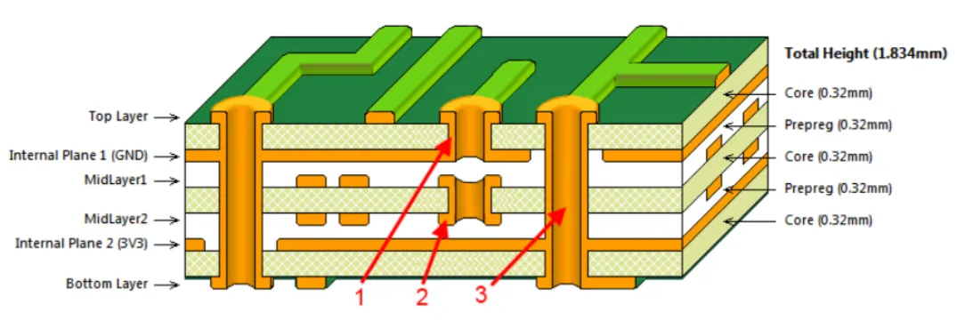
A PCB stackup refers to the arrangement of conductive and insulating layers in a multi-layer board. A typical 6-layer PCB stackup, for example, might include two signal layers on the top and bottom, with internal ground and power planes for stability. The goal of multi-layer PCB stackup DFM is to create a design that balances electrical performance with manufacturability.
DFM considerations in stackup design start with selecting the right materials and layer count. For instance, using standard dielectric materials with known properties ensures consistent manufacturing results. Additionally, engineers must plan the layer stack to avoid issues like warping or uneven thickness, which can occur if layers are not balanced properly. A poorly balanced stackup might have more copper on one side, leading to stress during fabrication. DFM guidelines recommend distributing copper evenly across layers to prevent such problems.
Another key DFM factor is minimizing the number of layers while meeting design requirements. Each additional layer increases manufacturing complexity and cost. By optimizing the stackup early, designers can avoid over-engineering and keep production efficient.
DFM for Impedance Control: Ensuring Signal Accuracy
Impedance control is vital for high-speed circuits, where signals must travel without distortion. In a multi-layer PCB, impedance depends on trace width, dielectric thickness, and the proximity of ground planes. DFM for impedance control focuses on creating a stackup that makes it easy to achieve and maintain the desired impedance values during manufacturing.
For example, a common target impedance for high-speed signals is 50 ohms. To achieve this, designers might place signal layers close to a ground plane, using a dielectric thickness of around 4-5 mils (0.1-0.13 mm) to control the impedance. DFM principles suggest using standard dielectric thicknesses and materials that manufacturers can reliably produce. This avoids variations in impedance that could occur if custom materials are used, which might not be consistently available or may lead to higher costs.
Additionally, DFM recommends maintaining consistent trace widths and spacing across the board. Variations in manufacturing can alter impedance if traces are not designed with tolerances in mind. By following DFM guidelines, engineers can ensure that impedance remains within acceptable limits, typically ±10% of the target value, even with minor production variations.
DFM for EMI Reduction: Minimizing Interference
Electromagnetic Interference (EMI) is a common challenge in multi-layer PCBs, especially in high-frequency applications. EMI can disrupt signal integrity and cause devices to fail regulatory standards. DFM for EMI reduction focuses on stackup designs that naturally suppress interference while being easy to manufacture.
One effective DFM strategy is to place ground planes adjacent to signal layers. This creates a shielding effect, reducing the chance of EMI radiating from high-speed traces. For instance, in a 4-layer PCB, a common stackup might be signal-ground-power-signal. This arrangement ensures that each signal layer is shielded by a ground or power plane, cutting down on crosstalk and external interference.
DFM also emphasizes proper layer spacing to avoid issues during fabrication. If layers are too close, manufacturers may struggle to maintain consistent dielectric thickness, leading to potential EMI problems. A practical DFM tip is to use standard spacing values, like 10 mils (0.25 mm) between layers, to ensure manufacturability while keeping EMI in check.
Finally, DFM encourages designers to avoid unnecessary vias or cutouts in ground planes, as these can create gaps that allow EMI to escape. By keeping ground planes intact and uniform, the stackup design remains both effective and manufacturable.
DFM for Signal Integrity: Maintaining Data Accuracy
Signal integrity refers to the ability of a signal to travel from source to destination without distortion or loss. In multi-layer PCBs, factors like crosstalk, reflections, and noise can degrade signal integrity, especially at high speeds (e.g., above 1 GHz). DFM for signal integrity ensures that the stackup design supports clean signal transmission while being practical for production.
A key DFM approach is to route high-speed signals on inner layers, sandwiched between ground planes. This reduces exposure to external noise and minimizes crosstalk. For example, in an 8-layer PCB, critical signals might be placed on layers 3 and 6, with ground planes on layers 2, 4, 5, and 7. This setup provides shielding and helps maintain signal quality.
DFM also considers manufacturing tolerances when planning trace lengths and spacing. If traces are too close, slight misalignments during production can cause crosstalk. A DFM-friendly design might specify a minimum spacing of 5 mils (0.13 mm) between high-speed traces to account for fabrication variations. This ensures signal integrity without requiring overly precise manufacturing, which can drive up costs.
Lastly, DFM suggests matching trace lengths for differential pairs to avoid timing mismatches. By designing with standard manufacturing capabilities in mind, engineers can ensure that signal integrity is preserved across the entire production run.
DFM for Layer Balancing: Preventing Manufacturing Defects
Layer balancing is a critical aspect of multi-layer PCB stackup design. If the layers are not balanced in terms of copper distribution or thickness, the board can warp or twist during manufacturing due to uneven thermal expansion. DFM for layer balancing focuses on creating a symmetrical stackup that minimizes stress and ensures a flat, reliable board.
For instance, in a 6-layer PCB, a balanced stackup might arrange layers as signal-ground-power-power-ground-signal. This symmetry ensures that copper and dielectric materials are distributed evenly, reducing the risk of warping. DFM guidelines recommend matching the copper weight (e.g., 1 oz or 0.035 mm per square foot) on corresponding layers to maintain balance.
Another DFM tip is to avoid placing high-density signal layers on one side of the board while leaving the other side sparse. This imbalance can cause mechanical stress during lamination. Instead, designers should distribute high-density areas evenly or add dummy copper fills to balance the design. These fills don’t affect electrical performance but help maintain structural integrity during production.
By following DFM principles for layer balancing, engineers can prevent costly manufacturing defects and ensure the final PCB meets both performance and quality standards.
Practical Tips for Applying DFM in Multi-Layer PCB Stackup Design
Now that we’ve covered the key areas where DFM impacts multi-layer PCB stackup design, here are some actionable tips to implement in your next project:
- Collaborate Early with Manufacturers: Share your stackup design with your fabrication partner before finalizing it. They can provide feedback on material availability and manufacturing constraints.
- Use Standard Materials: Opt for widely available dielectric materials and copper weights to avoid delays or cost overruns during production.
- Simulate Your Design: Use simulation tools to test impedance, EMI, and signal integrity before manufacturing. This helps catch potential issues early.
- Keep It Simple: Avoid overcomplicating the stackup with unnecessary layers or custom configurations. Simplicity often leads to better manufacturability.
- Document Thoroughly: Include detailed notes on layer arrangement, impedance targets, and critical design rules in your fabrication files to ensure clarity during production.
Conclusion: Why DFM is Essential for Multi-Layer PCB Success
Designing a multi-layer PCB stackup is a balancing act between electrical performance and manufacturing practicality. By integrating Design for Manufacturability (DFM) into the process, engineers can address critical challenges like impedance control, EMI reduction, signal integrity, and layer balancing. A well-executed DFM approach not only ensures that the PCB performs as intended but also reduces production costs and prevents delays.
Whether you’re working on a 4-layer board for a simple device or a 12-layer design for a high-speed application, applying DFM principles from the start will set you up for success. By focusing on manufacturable designs, you can create multi-layer PCBs that meet the highest standards of quality and reliability. So, the next time you plan a stackup, keep DFM at the forefront to achieve the best possible outcome for your project.


