 ALLPCB


Designing multi-layer printed circuit boards (PCBs) can be a complex task, but with the right Design for Manufacturability (DFM) strategies, you can significantly reduce costs and improve manufacturing efficiency. By focusing on DFM for multi-layer PCB cost reduction, you can streamline production processes, minimize errors, and ensure high-quality results without breaking the bank. In this comprehensive guide, we’ll dive into actionable DFM techniques tailored for multi-layer PCBs, covering key areas like component placement, material selection, and panelization. Whether you’re an engineer or a project manager, this post will provide practical insights to optimize your designs for PCB manufacturing cost DFM.
What is DFM and Why Does It Matter for Multi-Layer PCBs?
Design for Manufacturability (DFM) is a set of guidelines and practices that ensure a product’s design is optimized for efficient and cost-effective production. For multi-layer PCBs, which often involve intricate layouts with multiple layers of conductive traces and insulating materials, DFM is critical. These boards are used in advanced electronics like smartphones, medical devices, and automotive systems, where precision and reliability are non-negotiable.
Applying DFM principles early in the design phase helps identify potential manufacturing challenges before they become costly problems. This approach not only lowers production expenses but also reduces time-to-market and improves product quality. Let’s explore how focusing on DFM for multi-layer PCB cost reduction can transform your manufacturing process.
Key DFM Strategies for Multi-Layer PCB Cost Reduction
To achieve cost-effective manufacturing, you need to focus on specific DFM techniques tailored for multi-layer PCBs. Below, we break down the most impactful strategies, including component placement, material selection, and panelization, to help you optimize your designs for PCB manufacturing cost DFM.
1. Component Placement DFM: Streamlining Assembly
Component placement is one of the first areas to address when optimizing a multi-layer PCB for manufacturability. Poor placement can lead to assembly errors, increased production time, and higher costs. Here’s how to apply component placement DFM effectively:
- Group Similar Components: Place components with similar functions or assembly requirements together. For instance, grouping surface-mount components on one side of the board can reduce the need for multiple assembly passes, cutting down on labor and machine setup costs.
- Maintain Clear Spacing: Ensure adequate spacing between components to avoid soldering issues or interference during assembly. A minimum spacing of 0.1 mm between small components like 0402 resistors can prevent bridging during reflow soldering.
- Optimize for Automation: Align components in a grid pattern to support automated pick-and-place machines. Consistent orientation (e.g., all capacitors facing the same direction) can reduce programming time and errors during assembly.
- Avoid Overcrowding: Overcrowding on outer layers can complicate routing on inner layers. Distribute components evenly to balance thermal and mechanical stress, which also aids in maintaining signal integrity across high-speed traces.
By focusing on these component placement DFM practices, you can minimize assembly errors and reduce manufacturing costs by up to 15%, depending on the complexity of your design.
2. Material Selection DFM: Balancing Cost and Performance
The materials you choose for your multi-layer PCB have a direct impact on both cost and manufacturability. With material selection DFM, the goal is to select materials that meet performance requirements while keeping production expenses low. Here’s how to approach this:
- Choose Standard Materials: Opt for widely available materials like FR-4 for the substrate unless your design requires high-frequency performance. FR-4 is cost-effective and compatible with most standard manufacturing processes, often costing 20-30% less than specialized laminates.
- Match Copper Thickness to Current Needs: Use the appropriate copper weight for your design’s current-carrying requirements. For example, 1 oz/ft2 copper is sufficient for most low-power applications, while 2 oz/ft2 may be needed for high-current traces. Over-specifying copper increases material costs unnecessarily.
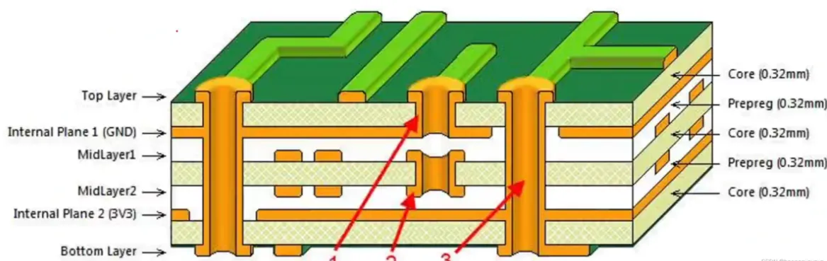
- Consider Layer Stackup Early: Plan your layer stackup to minimize the number of layers while meeting signal integrity needs. Reducing from 8 to 6 layers, for instance, can cut material and processing costs by 10-20%, depending on the board size.
- Avoid Exotic Finishes Unless Necessary: While finishes like ENEPIG (Electroless Nickel Electroless Palladium Immersion Gold) offer excellent reliability, they are expensive. For many applications, a standard HASL (Hot Air Solder Leveling) finish can suffice at a fraction of the cost.
Effective material selection DFM ensures that you’re not overspending on materials while still meeting the electrical and thermal demands of your design. Always consult with your manufacturing partner to confirm material availability and compatibility with their processes.
3. Panelization DFM: Maximizing Production Efficiency
Panelization refers to arranging multiple PCB designs on a single manufacturing panel to optimize material usage and streamline production. Proper panelization DFM can significantly lower costs, especially for high-volume runs. Here’s how to implement it:
- Standardize Panel Sizes: Use standard panel sizes (e.g., 18” x 24”) to maximize compatibility with manufacturing equipment. Custom sizes often lead to wasted material and higher setup costs.
- Optimize Board Orientation: Arrange boards on the panel to minimize wasted space. For example, rotating smaller boards by 90 degrees can sometimes fit an additional unit on the panel, reducing material costs by 5-10%.
- Use Breakaway Tabs or V-Scoring: Design breakaway tabs or V-scoring lines to separate individual boards after manufacturing. V-scoring is often cheaper for straight edges, while mouse bites (small perforated tabs) work well for irregular shapes.
- Include Fiducials and Tooling Holes: Add fiducial markers and tooling holes on the panel for precise alignment during assembly. This reduces errors in automated processes, saving time and minimizing scrap rates.
By focusing on panelization DFM, you can make the most of every manufacturing run, cutting down on material waste and reducing per-unit costs. For large orders, efficient panelization can lead to savings of up to 15% on material costs alone.
Additional DFM Tips for Multi-Layer PCB Cost Reduction
Beyond the core areas of component placement, material selection, and panelization, there are other DFM practices that can further optimize your multi-layer PCB designs for PCB manufacturing cost DFM. Here are some additional strategies to consider:
- Minimize Via Usage: Excessive vias, especially microvias, can increase drilling and plating costs. Use through-hole vias where possible, as they are cheaper to produce. For high-density designs, limit microvias to outer layers to reduce complexity and cost.
- Simplify Trace Routing: Keep trace widths and spacing consistent with manufacturing capabilities. For example, a minimum trace width of 6 mils and spacing of 6 mils is often achievable with standard processes, avoiding the need for premium fabrication services.
- Design for Testability: Include test points for critical nets to simplify in-circuit testing (ICT). This reduces debugging time during production and prevents costly rework. Ensure test points are accessible and spaced at least 0.1 inches apart for probe accuracy.
- Avoid Tight Tolerances Unless Necessary: Specifying overly tight tolerances for dimensions or impedance can drive up costs. For instance, a standard impedance tolerance of ±10% is often sufficient for most applications, while ±5% may require specialized processes and increase costs by 20% or more.
Implementing these additional DFM techniques can further enhance manufacturing efficiency and contribute to significant DFM for multi-layer PCB cost reduction.
Benefits of DFM for Multi-Layer PCB Manufacturing
Adopting DFM practices for multi-layer PCB design offers several advantages that go beyond just cost savings. Here are some key benefits:
- Reduced Production Errors: DFM identifies potential issues like insufficient clearances or incompatible materials before manufacturing begins, minimizing costly mistakes.
- Faster Time-to-Market: Streamlined designs are easier to produce, reducing lead times and helping you get products to market quicker.
- Improved Product Quality: DFM ensures that designs are robust and reliable, leading to fewer defects and higher customer satisfaction.
- Lower Overall Costs: From material savings to reduced rework, DFM practices can lower total production costs by 10-30%, depending on the project scope.
Collaborating with Your Manufacturing Partner for DFM Success
One of the most effective ways to ensure DFM success is to work closely with your manufacturing partner from the start. Share your design files early and request feedback on potential manufacturability issues. Many manufacturers offer free DFM checks to identify problems like insufficient annular rings or unsupported trace widths before production begins.
Additionally, provide detailed documentation, including layer stackup diagrams, bill of materials (BOM), and assembly drawings. Clear communication helps avoid misunderstandings and ensures that your design aligns with the manufacturer’s capabilities. This collaborative approach is essential for achieving PCB manufacturing cost DFM goals.
Conclusion: Achieving Cost-Effective Multi-Layer PCB Manufacturing with DFM
Optimizing multi-layer PCB designs for manufacturability is a powerful way to reduce costs and improve production efficiency. By focusing on DFM for multi-layer PCB cost reduction, you can address key areas like component placement DFM, material selection DFM, and panelization DFM to create designs that are easier and cheaper to produce. These strategies, combined with early collaboration with your manufacturing partner, ensure that your PCBs meet performance requirements without unnecessary expenses.
Start implementing these DFM practices in your next project to experience the benefits of streamlined manufacturing and significant cost savings. With the right approach to PCB manufacturing cost DFM, you can deliver high-quality multi-layer PCBs that meet both technical and budgetary goals.


