ALLPCB


Have you ever received a printed circuit board (PCB) only to find that the silkscreen markings are missing, incomplete, or peeling off? This issue, often tied to problems like missing silkscreen markings, incomplete silkscreen layers, or silkscreen adhesion problems, can create significant challenges during assembly, testing, and maintenance. In this blog post, we’ll dive into what happens when the silkscreen vanishes from your PCB, why it matters, and how to prevent issues related to PCB silkscreen durability and silkscreen material choices. Let’s explore the impact of these problems and offer practical solutions to ensure your boards are labeled clearly and reliably.
What Is a PCB Silkscreen and Why Does It Matter?
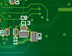
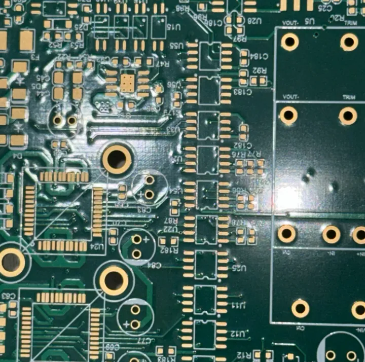
The silkscreen layer on a PCB is the printed text, symbols, and markings on the board’s surface. These labels typically include component references (like R1 for a resistor), polarity indicators, test points, and other essential information. Made from non-conductive epoxy ink, the silkscreen is applied during manufacturing to guide assembly, testing, and troubleshooting processes.
Without a clear and durable silkscreen, identifying components or understanding their orientation becomes a guessing game. This can lead to errors during assembly, delays in production, and even costly rework. Issues like missing silkscreen markings or an incomplete silkscreen layer can disrupt workflows, while poor silkscreen adhesion or low durability can cause labels to wear off over time, especially under harsh conditions.
The Consequences of Missing Silkscreen Markings on Your PCB
When silkscreen markings are missing or incomplete, the impact can be felt across multiple stages of a PCB’s lifecycle. Here’s a breakdown of the problems that arise:
1. Assembly Errors
During assembly, technicians rely on silkscreen labels to place components correctly. Missing silkscreen markings can lead to incorrect placements, such as a capacitor installed backward or a wrong resistor value used. For high-density boards with hundreds of components, even a single mistake can render the entire board unusable, leading to scrap rates as high as 5-10% in some production runs if errors go undetected.
2. Increased Debugging Time
Testing and debugging a PCB without silkscreen labels is like solving a puzzle with missing pieces. Engineers must refer to schematics or layout files to identify components, which can double or triple the time spent on troubleshooting. For complex designs, this delay can add hours or even days to a project timeline.
3. Maintenance Challenges
Once a PCB is in the field, maintenance teams depend on silkscreen markings to identify components for repairs or replacements. An incomplete silkscreen layer means technicians may struggle to locate specific parts, increasing downtime for the end user. In critical applications like medical or automotive systems, this can have serious consequences.
Common Causes of Silkscreen Issues on PCBs
Understanding why silkscreen problems occur is the first step to preventing them. Here are the most common issues related to missing silkscreen markings, incomplete layers, adhesion problems, and durability concerns:
1. Incomplete Silkscreen Layer During Manufacturing
An incomplete silkscreen layer often results from errors in the design file or manufacturing process. If the silkscreen data is missing from the Gerber files submitted for production, the markings won’t be printed on the board. Additionally, if the printing process is rushed or misaligned, sections of the silkscreen may be omitted, leaving critical labels absent.
2. Silkscreen Adhesion Problems
Silkscreen adhesion problems occur when the ink fails to bond properly to the PCB surface. This can happen due to poor surface preparation, such as residual flux or contaminants on the board before printing. Certain solder mask colors or finishes may also reduce adhesion, causing the silkscreen to peel or flake off during handling or soldering. For instance, some studies suggest that adhesion issues are more common with certain matte finishes compared to glossy ones, with failure rates increasing by up to 15% under thermal stress.
3. PCB Silkscreen Durability Issues
PCB silkscreen durability is critical for long-term reliability. Low-quality ink or improper curing during manufacturing can lead to markings that fade, scratch off, or degrade under environmental stress like heat, humidity, or chemical exposure. For boards used in industrial settings, where temperatures can exceed 85°C, durability issues can cause up to 20% of silkscreen markings to become illegible within a year if low-grade materials are used.
4. Poor Silkscreen Material Choices
The choice of silkscreen material plays a huge role in its performance. Standard non-conductive epoxy inks are designed to withstand soldering temperatures up to 260°C and resist corrosion. However, opting for cheaper or incompatible materials can compromise adhesion and durability. For example, some low-cost inks may not handle reflow soldering well, leading to cracking or peeling during assembly.
How Missing Silkscreen Markings Affect Production Costs
The financial impact of silkscreen issues can be significant, especially for large-scale production. Let’s break down the costs associated with missing or incomplete silkscreen layers:
- Rework and Scrap: Boards with missing silkscreen markings often require manual labeling or rework, adding labor costs. In severe cases, boards may need to be scrapped, with losses ranging from $5 to $50 per board depending on complexity.
- Production Delays: Identifying and fixing silkscreen errors can delay production schedules by days or weeks, impacting delivery timelines and potentially leading to penalties for late shipments.
- Customer Returns: If incomplete silkscreen layers lead to assembly errors that go unnoticed, defective products may reach customers, resulting in returns or warranty claims that can cost manufacturers thousands of dollars annually.
By addressing silkscreen issues early in the design and manufacturing process, companies can save on these hidden costs and maintain a reputation for quality.
Solutions to Prevent Silkscreen Problems on Your PCB
Preventing issues like missing silkscreen markings, adhesion problems, and durability concerns requires attention to design, material selection, and manufacturing practices. Here are actionable steps to ensure your PCB silkscreen remains clear and reliable:
1. Verify Silkscreen Data in Design Files
Before sending your design for manufacturing, double-check that the silkscreen layer is included in your Gerber files. Use design rule checks (DRC) in your CAD software to catch errors like missing labels or overlapping text. Ensure that all critical markings, such as component references and polarity indicators, are present and legible.
2. Choose High-Quality Silkscreen Materials
Work with your manufacturing partner to select silkscreen materials that offer strong adhesion and durability. Opt for industry-standard epoxy inks that can withstand high temperatures and environmental stress. If your PCB will be used in harsh conditions, consider requesting enhanced curing processes to improve ink bonding and longevity.
3. Optimize Silkscreen Color and Contrast
Select a silkscreen color that contrasts well with your solder mask for maximum visibility. For example, white silkscreen on a green solder mask is a common choice for its clarity. Avoid colors with known adhesion issues, as some pigments may not bond as effectively to certain surfaces, increasing the risk of peeling.
4. Test for Silkscreen Adhesion and Durability
Request adhesion and durability testing during the prototyping phase. Tests like tape adhesion (where tape is applied and removed to check if ink peels off) and thermal cycling (exposing the board to temperature extremes) can identify potential issues before full-scale production. Aim for silkscreen durability that maintains legibility even after 500 hours of exposure to 85°C and 85% humidity, a common benchmark for industrial applications.
5. Collaborate with Your Manufacturer
Communicate clearly with your manufacturing partner about your silkscreen requirements. Provide detailed specifications for ink type, curing conditions, and placement accuracy. Request samples or first-article inspections to verify that the silkscreen meets your expectations before proceeding with a full production run.
Best Practices for Designing a Reliable Silkscreen Layer
Designing a silkscreen layer that avoids issues like incomplete markings or adhesion problems starts with following industry best practices. Here are some tips to keep in mind:
- Keep Text Legible: Use a minimum font size of 6 points (about 1.5mm in height) to ensure readability, even under magnification. Avoid overly complex fonts that may blur during printing.
- Avoid Overcrowding: Place silkscreen markings away from densely populated areas to prevent overlap with components or vias. Leave at least 0.2mm of clearance around pads and traces.
- Prioritize Key Information: Focus on essential labels like component designators and polarity markers. Avoid cluttering the board with non-critical information that could obscure important details.
- Account for Manufacturing Tolerances: Design with manufacturing limitations in mind. Silkscreen alignment can vary by ±0.1mm, so ensure markings are not placed too close to edges or critical features.
Conclusion: Don’t Let Missing Silkscreen Markings Derail Your Project
The silkscreen layer on your PCB may seem like a small detail, but its absence or poor quality can lead to major headaches. Missing silkscreen markings, incomplete silkscreen layers, silkscreen adhesion problems, and durability issues can disrupt assembly, increase costs, and delay projects. By understanding the causes of these problems and taking proactive steps—such as verifying design files, choosing high-quality silkscreen materials, and testing for durability—you can ensure your PCBs are labeled clearly and built to last.
At ALLPCB, we’re committed to delivering high-quality boards with reliable silkscreen markings that meet your needs. Whether you’re dealing with complex designs or high-volume production, our team is here to help you avoid the pitfalls of silkscreen issues. Focus on designing with precision, collaborate closely with your manufacturer, and prioritize durability to keep your projects on track.