 ALLPCB


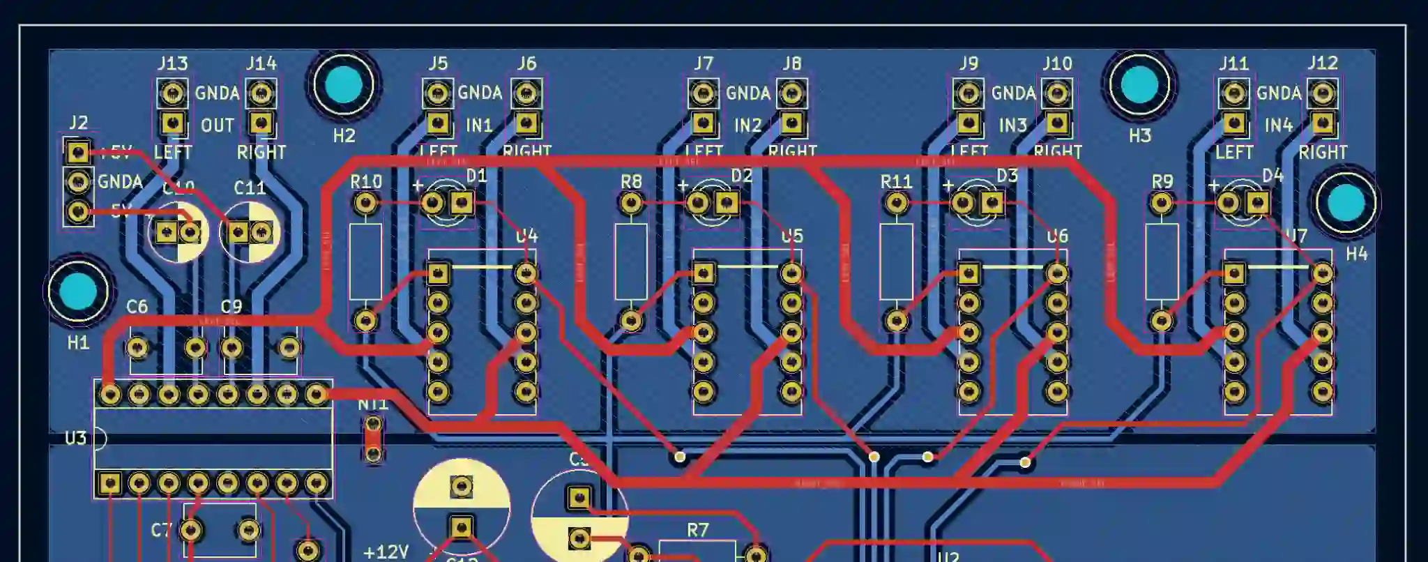
When designing an audio amplifier PCB, one critical factor often overlooked is trace width. So, how does trace width impact audio quality in amplifier PCBs? Simply put, trace width affects current carrying capacity, signal loss, impedance, and power delivery—all of which directly influence the clarity, strength, and fidelity of audio output. A poorly designed trace width can lead to distortion, noise, or even component failure, while an optimized width ensures clean sound and reliable performance.
In this comprehensive guide, we’ll dive deep into the relationship between trace width and audio quality in amplifier PCBs. We’ll explore how trace width impacts key electrical properties and provide practical tips for optimizing your PCB layout for superior sound. Whether you’re an audio engineer or a hobbyist, this post will equip you with the knowledge to design better audio amplifier PCBs.
Why Trace Width Matters in Audio Amplifier PCBs
Trace width refers to the thickness of the copper pathways on a printed circuit board (PCB) that carry electrical signals and power between components. In audio amplifier PCBs, these traces are responsible for delivering power to the amplifier circuit and transmitting audio signals with minimal interference or loss. If the trace width isn’t properly calculated, it can create bottlenecks in current flow, increase resistance, and degrade audio quality.
For audio applications, even small imperfections in signal transmission can result in noticeable distortion or noise. That’s why understanding and optimizing trace width is crucial for achieving high-fidelity sound. Let’s break down the specific ways trace width impacts audio quality, focusing on current carrying capacity, signal loss, impedance, and power delivery.
Trace Width and Current Carrying Capacity in Audio Amplifiers
Current carrying capacity is the amount of electrical current a trace can handle without overheating or failing. In audio amplifier PCBs, traces often carry significant current, especially in power supply lines feeding the amplifier stages. If a trace is too narrow, it can overheat due to high resistance, leading to voltage drops and potential damage to the PCB or components.
For example, a typical Class AB audio amplifier might require traces to handle currents of 2-5 amps or more during peak operation. According to standard PCB design guidelines, a trace width of 1.5 mm (60 mils) on a 1 oz copper layer can safely carry around 2.5 amps at a temperature rise of 10°C. For higher currents, wider traces or thicker copper layers (e.g., 2 oz) are necessary to prevent overheating.
When current carrying capacity is insufficient, the amplifier may experience power starvation, resulting in reduced output power and distorted audio. To avoid this, designers must calculate the required trace width based on the expected current load and ensure the PCB material can handle the thermal stress.
Practical Tip: Use online trace width calculators or IPC-2221 standards to determine the appropriate width for your current needs. Always add a safety margin of 20-30% to account for unexpected power spikes in audio applications.
Signal Loss and Its Effect on Audio Fidelity
Signal loss occurs when a trace’s resistance or other electrical properties degrade the audio signal as it travels through the PCB. In audio amplifier PCBs, signal loss can manifest as reduced volume, muffled sound, or loss of high-frequency details. Trace width plays a direct role in minimizing signal loss by reducing resistance and ensuring the signal maintains its integrity.
Narrow traces have higher resistance, which can attenuate audio signals, especially over longer distances. For instance, a trace with a width of 0.1 mm (4 mils) might be suitable for low-current digital signals, but it’s far too thin for analog audio signals, where resistance can cause noticeable degradation. Wider traces, such as 0.5 mm (20 mils) or more, are often recommended for audio signal paths to keep resistance low.
Additionally, signal loss can be exacerbated by poor layout practices, such as running audio traces near noisy power lines. Combining proper trace width with good routing techniques ensures minimal signal loss and preserves audio fidelity.
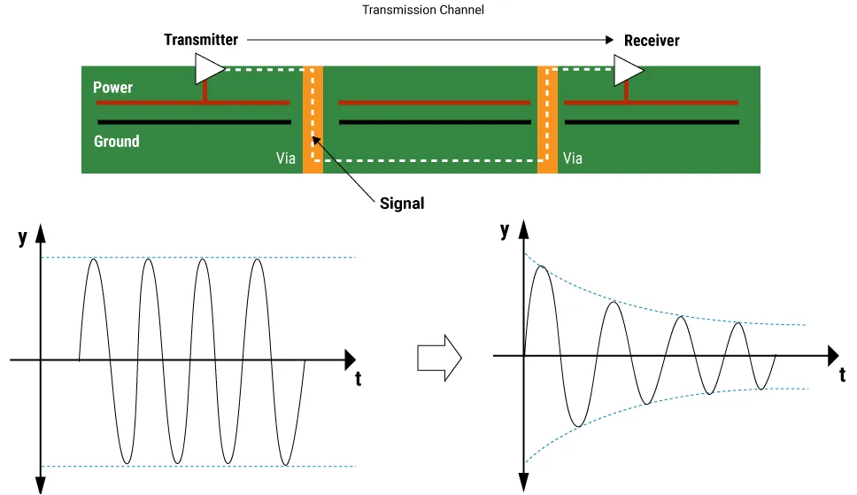
Impedance Control for Clean Audio Signals
Impedance is the measure of opposition to alternating current (AC) in a circuit, and it’s a critical factor in audio amplifier PCB design. Mismatched impedance between traces, components, and speakers can cause signal reflections, resulting in distortion or phase issues that degrade audio quality. Trace width directly affects impedance, as wider traces generally have lower impedance due to reduced resistance and inductance.
In high-frequency audio signals (e.g., above 10 kHz), controlling impedance becomes even more important. For example, a trace width of 0.8 mm (30 mils) on a standard FR-4 PCB with a 1.6 mm thickness might yield a characteristic impedance of around 50 ohms, which is often ideal for matching with audio components. If the trace is too narrow, the impedance increases, potentially causing signal mismatches and audible artifacts.
To achieve proper impedance control, designers must consider not only trace width but also trace spacing, dielectric material, and layer stack-up. Using simulation tools during the design phase can help predict and adjust impedance values for optimal audio performance.
Practical Tip: For critical audio signal paths, aim for consistent trace widths and avoid sharp corners or sudden changes in width, as these can disrupt impedance and introduce noise.
Power Delivery and Its Role in Audio Performance
Effective power delivery is the backbone of any audio amplifier PCB. Amplifiers require stable and sufficient power to drive speakers without distortion, and trace width plays a pivotal role in ensuring this. Narrow traces in power delivery lines can create voltage drops, especially during dynamic audio peaks when current demand spikes.
For instance, if a power trace is designed to handle only 1 amp but the amplifier demands 3 amps during a loud bass note, the resulting voltage drop can cause the amplifier to clip, producing harsh distortion. A wider trace, such as 2 mm (80 mils) or more for high-power lines, ensures that the voltage remains stable, allowing the amplifier to deliver clean, undistorted sound.
Power delivery issues are particularly noticeable in low-frequency audio, where high current is needed to reproduce deep bass tones. Designers should prioritize wider traces for power and ground lines, often using ground planes to further stabilize power delivery and reduce noise.
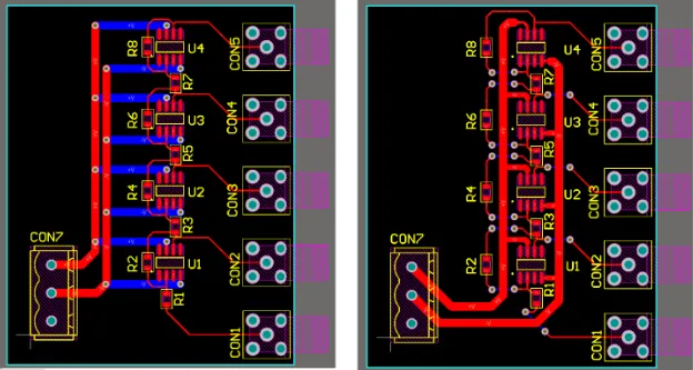
Balancing Trace Width with PCB Design Constraints
While wider traces are generally better for current carrying capacity, low signal loss, and stable power delivery, they come with trade-offs. Wider traces take up more space on the PCB, which can be problematic in compact designs or when routing multiple signals. Additionally, manufacturing costs may increase if wider traces require thicker copper layers or specialized materials.
To strike a balance, prioritize wider traces for high-current and power delivery paths while using narrower traces (e.g., 0.2-0.3 mm or 8-12 mils) for low-current audio signals where space is limited. It’s also helpful to use multi-layer PCBs for audio amplifiers, as they allow for dedicated power and ground planes, freeing up space on the signal layer for optimized trace routing.
Another consideration is manufacturability. Most PCB fabrication houses have minimum trace width and spacing requirements, often around 0.15 mm (6 mils) for standard processes. Ensure your trace widths comply with these limits to avoid production issues.
Tips for Optimizing Trace Width in Audio Amplifier PCBs
Designing an audio amplifier PCB with optimal trace width requires careful planning and attention to detail. Here are some actionable tips to help you achieve the best audio quality:
- Calculate Current Needs: Determine the maximum current for each trace, especially power lines, and use a trace width calculator to find the appropriate size. Add a safety margin for reliability.
- Minimize Signal Path Lengths: Keep audio signal traces as short as possible to reduce resistance and signal loss. Use wider traces (e.g., 0.5 mm or 20 mils) for longer runs if needed.
- Use Ground Planes: Incorporate a solid ground plane to reduce noise and improve power delivery. Connect critical components directly to the ground plane with vias.
- Separate Power and Signal Traces: Route power traces away from sensitive audio signal traces to prevent interference. Use wider traces for power to ensure stable voltage.
- Test and Simulate: Use PCB design software with simulation features to test impedance and signal integrity before manufacturing. Adjust trace widths as needed based on simulation results.
Common Mistakes to Avoid with Trace Width in Audio PCBs
Even experienced designers can make mistakes when it comes to trace width in audio amplifier PCBs. Here are some common pitfalls to watch out for:
- Underestimating Current Requirements: Failing to account for peak current demands can lead to overheating and failure. Always design for the worst-case scenario.
- Using Uniform Trace Widths: Not all traces need the same width. Use wider traces for power and narrower ones for signals to optimize space and performance.
- Ignoring Impedance Matching: Inconsistent trace widths can disrupt impedance, causing signal reflections and audio distortion. Maintain uniform widths for critical signal paths.
- Overlooking Thermal Management: High-current traces generate heat. Ensure proper trace width and consider adding thermal vias or heat sinks if needed.
How Trace Width Impacts Overall Audio System Design
Trace width doesn’t just affect the PCB itself—it influences the entire audio system. A well-designed PCB with optimized trace widths ensures that the amplifier can deliver its full potential, providing clear and powerful sound to speakers. On the other hand, poor trace width choices can bottleneck performance, leading to an underwhelming listening experience no matter how high-quality the other components are.
For example, in a home theater system, an audio amplifier PCB with inadequate trace width might struggle to deliver the dynamic range needed for cinematic sound effects. Conversely, a properly designed PCB can handle sudden volume changes and deep bass without distortion, enhancing the overall audio experience.
Conclusion: Designing for Audio Excellence with Proper Trace Width
The impact of trace width on audio quality in amplifier PCBs cannot be overstated. By carefully considering current carrying capacity, signal loss, impedance, and power delivery, you can design PCBs that deliver exceptional audio performance. Wider traces are essential for high-current and power lines to prevent overheating and voltage drops, while appropriately sized traces for signal paths minimize loss and maintain fidelity.
Optimizing trace width is both a science and an art. It requires balancing electrical requirements with space constraints and manufacturing capabilities. With the tips and insights provided in this guide, you’re well-equipped to tackle the challenges of audio amplifier PCB design and achieve outstanding sound quality in your projects.
Remember, every detail matters in audio design. Take the time to calculate, simulate, and refine your trace widths, and you’ll hear the difference in every note. For high-quality PCB manufacturing and design support tailored to audio applications, trust a reliable partner to bring your vision to life.


