 ALLPCB


For printed circuit board (PCB) designers, achieving precise impedance control is critical for ensuring signal integrity, especially in high-speed and high-frequency applications. However, PCB manufacturing tolerances can significantly impact impedance, leading to variations that affect performance. Factors such as etching, plating, impedance variation, and process control play a key role in this challenge. In this blog, we’ll explore how these tolerances influence impedance control and provide actionable insights to help designers navigate these issues effectively.
Whether you're working on RF circuits, digital designs, or other advanced applications, understanding the relationship between manufacturing tolerances and impedance is essential. Let’s dive into the details of how these factors interact and what you can do to minimize risks during the design and fabrication process.
Understanding Impedance Control in PCB Design
Impedance control refers to the practice of designing PCB traces to maintain a specific electrical impedance, ensuring that signals travel without unwanted reflections or losses. This is particularly important in high-speed circuits where even small deviations can cause signal degradation. The target impedance for a trace is often calculated based on the application, with common values like 50 ohms for RF signals or 100 ohms for differential pairs in digital systems.
However, achieving consistent impedance isn’t just a matter of design. Manufacturing tolerances introduce variations that can push impedance values outside the desired range, leading to performance issues. Industry standards often specify a tolerance of ±10% for controlled impedance, though tighter tolerances like ±5% or ±3% may be necessary for critical applications such as 5G or high-frequency RF designs.
Key Manufacturing Tolerances Affecting Impedance Control
Several aspects of PCB fabrication directly influence impedance. Below, we break down the primary factors—etching, plating, dielectric thickness, and overall process control—and explain their impact on impedance variation.
1. Etching Tolerances and Trace Width Variations
The etching process shapes the copper traces on a PCB by removing unwanted copper from the board. While this process is essential for defining trace geometry, it introduces tolerances that affect trace width and, consequently, impedance. If a trace is designed to be 10 mils wide for a 50-ohm impedance, a ±10% tolerance means the actual width could vary between 9 and 11 mils. Even this small deviation can alter impedance by several ohms, disrupting signal integrity.
Etching variations often stem from factors like undercut (where the etchant removes more copper than intended) or inconsistencies in the photomask used to define the trace pattern. To mitigate these issues, manufacturers often apply engineering compensation during the design of photomasks to account for expected etch errors. As a designer, specifying tight tolerances for trace width and collaborating with your fabricator to understand their etching capabilities can help maintain consistency.

2. Plating Tolerances and Copper Thickness
Plating adds a layer of copper or other conductive material to the traces and vias after etching. The thickness of this plated copper directly impacts the trace’s cross-sectional area, which in turn affects impedance. For instance, if a design assumes a copper thickness of 1 oz/ft2 (approximately 35 microns), but plating results in a thickness of 1.2 oz/ft2 due to tolerance variations, the impedance could drop lower than expected.
Plating tolerances are influenced by factors like the plating bath’s chemical composition, current density, and process duration. Variations in copper thickness can be particularly problematic for high-frequency designs, where skin effect (the tendency of current to flow near the surface of a conductor) amplifies the impact of thickness changes. Designers should specify acceptable copper thickness ranges and work with manufacturers to ensure tight control over plating processes.
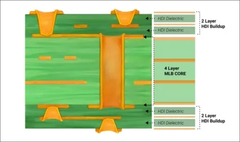
3. Dielectric Thickness and Material Tolerances
The dielectric material between conductive layers of a PCB also plays a crucial role in impedance control. The thickness and dielectric constant (Dk) of this material determine how much impedance a trace will have. For example, in a microstrip configuration, a thicker dielectric increases impedance, while a thinner dielectric decreases it. If a design targets a dielectric thickness of 10 mils for a specific impedance, but manufacturing tolerances result in a thickness of 9.5 or 10.5 mils, the impedance can shift by 2-3 ohms or more.
Dielectric thickness variations often occur during lamination, where factors like press flatness and resin content in prepreg materials can lead to inconsistencies. Additionally, the dielectric constant of materials can vary slightly from batch to batch or change with temperature (typically by 0.5-1% per 10°C). Designers should select materials with stable properties and account for these tolerances when calculating impedance using tools or formulas.
4. Process Control and Manufacturing Consistency
Even with precise designs, poor process control during manufacturing can introduce unpredictable impedance variation. This includes inconsistencies in etching, plating, lamination, and even environmental factors like temperature and humidity in the fabrication facility. For instance, uneven etching across a board can result in some traces being over-etched while others are under-etched, leading to impedance mismatches across the same PCB.
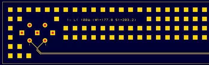
Effective process control involves rigorous quality checks, such as using test coupons on each panel to measure impedance after fabrication. These coupons are small test structures that mimic the design’s critical traces and are measured to ensure they fall within the specified tolerance (e.g., ±10%). As a designer, requesting detailed feedback from your fabricator about their process control measures can help ensure consistency and reduce impedance deviations.
How Impedance Variation Impacts Signal Integrity
When manufacturing tolerances lead to impedance variations, the consequences for signal integrity can be significant. In high-speed digital circuits operating at speeds above 1 GHz, impedance mismatches can cause signal reflections, leading to data errors or reduced system reliability. For RF applications, even a 5% deviation from the target impedance (e.g., 50 ohms to 52.5 ohms) can result in power loss and degraded performance.
Consider a differential pair in a high-speed design with a target impedance of 100 ohms. If manufacturing tolerances cause one trace to have an impedance of 95 ohms and the other 105 ohms, the mismatch can introduce noise and crosstalk, compromising the signal. Understanding these risks highlights the importance of accounting for PCB manufacturing tolerances early in the design phase.
Strategies for Designers to Mitigate Impedance Variations
While manufacturing tolerances are inevitable, designers can take proactive steps to minimize their impact on impedance control. Here are some practical strategies to consider during the design and fabrication process:
1. Design with Tolerances in Mind
Start by incorporating expected manufacturing tolerances into your impedance calculations. For example, if trace width tolerance is ±10%, simulate impedance for the minimum and maximum widths (e.g., 9 mils and 11 mils for a 10-mil trace) to ensure the design remains functional across this range. Use PCB design software with built-in impedance calculators to model these variations accurately.
2. Specify Tight Tolerances Where Necessary
For critical applications, request tighter tolerances from your fabricator, such as ±5% for trace width or dielectric thickness. Be aware that tighter tolerances may increase production costs, so balance performance needs with budget constraints. Clearly communicate these requirements in your fabrication notes to avoid misunderstandings.
3. Collaborate with Your Manufacturer
Engage with your PCB fabricator early in the design process to understand their specific capabilities and tolerances for etching, plating, and other processes. Request stack-up recommendations and impedance control guidelines tailored to their equipment and materials. This collaboration can help align your design with their manufacturing strengths, reducing the risk of impedance issues.
4. Use Test Structures and Validation
Include test structures or coupons in your PCB design to allow for impedance measurement after fabrication. These structures should replicate the critical traces in your design and be placed on the same panel to reflect actual manufacturing conditions. Reviewing the measured impedance data can help identify and address variations before full production.
5. Select Materials with Stable Properties
Choose dielectric materials with consistent dielectric constants and minimal variation under temperature changes. High-quality materials may cost more but offer better reliability for impedance control. Specify these materials in your design files and confirm with your fabricator that they can source and process them correctly.
The Role of Advanced Tools in Managing Tolerances
Modern PCB design tools can significantly aid in managing impedance variation caused by manufacturing tolerances. These tools allow designers to simulate impedance based on different stack-ups, trace geometries, and material properties. Some software even offers features to input manufacturing tolerances directly into simulations, providing a realistic view of how variations might affect performance.
For instance, when designing a 50-ohm microstrip line, you can use these tools to calculate impedance using formulas like:
Z = (87 / √(Er + 1.41)) * ln(5.98H / (0.8W + T))
Where:
- Z is the impedance (ohms)
- Er is the dielectric constant
- H is the dielectric height (mils)
- W is the trace width (mils)
- T is the trace thickness (mils)
By adjusting variables like W and H within the expected tolerance range, you can predict impedance shifts and adjust your design accordingly. Leveraging such tools ensures that your design is robust against manufacturing variations.
Conclusion: Balancing Design and Manufacturing for Optimal Impedance Control
Achieving reliable impedance control in PCB design requires a deep understanding of PCB manufacturing tolerances and their impact on critical processes like etching, plating, and process control. Variations in trace width, copper thickness, and dielectric properties can lead to impedance variation, affecting signal integrity and overall system performance. However, by designing with tolerances in mind, specifying requirements clearly, and collaborating closely with your fabricator, you can minimize these risks and ensure consistent results.
At ALLPCB, we understand the challenges of maintaining precise impedance control in high-speed and high-frequency designs. Our advanced manufacturing capabilities and strict process control measures are designed to help you achieve the tight tolerances needed for your projects. By partnering with us, you gain access to expertise and tools that support your design goals, from concept to production.
Navigating the complexities of impedance control doesn’t have to be overwhelming. With the right strategies and support, you can create designs that perform reliably, even in the face of manufacturing variations. Keep these insights in mind as you tackle your next PCB project, and you’ll be well-equipped to handle the challenges of impedance control.


