 ALLPCB


In the fast-paced world of electronics, ensuring high-quality performance in printed circuit boards (PCBs) is more important than ever. One advanced technique that stands out in modern PCB manufacturing is backdrilling, also known as controlled depth drilling. This process is a game-changer for high-speed designs, as it directly improves signal integrity by addressing common issues like signal reflections and distortions. If you're looking to optimize your PCB for high-speed applications, backdrilling could be the solution you need.
In this comprehensive guide, we'll dive deep into the benefits of backdrilling in modern PCB manufacturing. We'll explore how it enhances signal integrity, its role in high-speed design, and why it’s becoming a standard in the industry. Whether you're an engineer or a designer, this post will provide actionable insights into controlled depth drilling and its impact on your projects.
What Is Backdrilling in PCB Manufacturing?
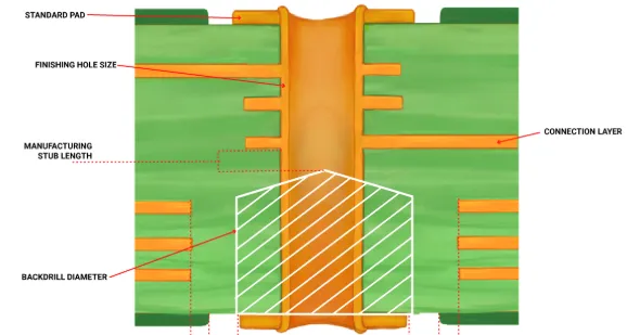
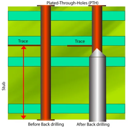
Backdrilling is a specialized technique used during PCB manufacturing to remove unused portions of copper from plated through-hole (PTH) vias. These unused sections, known as via stubs, can act as tiny antennas that cause signal reflections and distortions in high-speed designs. By using controlled depth drilling, manufacturers drill into the PCB from the back side to eliminate these stubs without affecting the functional part of the via.
In high-speed designs, where data rates can exceed 10 Gbps, even small imperfections like via stubs can lead to significant signal loss. Backdrilling targets this problem directly, ensuring cleaner signal transmission. This process is especially critical in multilayer PCBs, where signals often travel through multiple layers, increasing the risk of interference.
Why Signal Integrity Matters in High-Speed Design
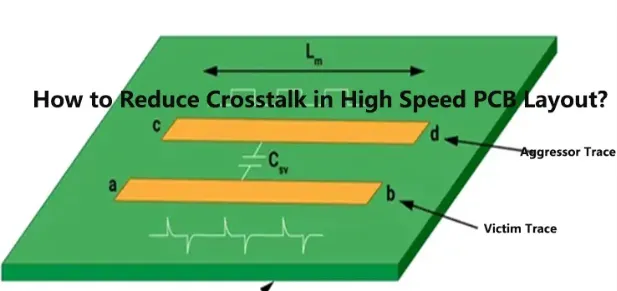
Signal integrity refers to the quality of an electrical signal as it travels through a PCB. In high-speed designs, maintaining signal integrity is crucial because even minor disruptions can lead to data errors or system failures. Common issues that degrade signal integrity include crosstalk, impedance mismatches, and reflections caused by via stubs.
For instance, in applications like 5G communication or high-performance computing, signal speeds often reach 25 Gbps or higher. At these rates, a via stub as short as 0.5 mm can create enough reflection to distort the signal. This is where backdrilling shines, as it minimizes these risks by physically removing the problematic stub, allowing the signal to travel with less interference.
By focusing on signal integrity, designers can achieve faster, more reliable performance in their PCBs. Backdrilling is a proven method to support this goal, making it a valuable tool in modern electronics manufacturing.
Key Benefits of Backdrilling in PCB Manufacturing
Backdrilling offers several advantages that make it essential for high-speed PCB designs. Below, we’ll break down the most significant benefits, supported by practical examples and data where applicable.
1. Improved Signal Integrity
As mentioned earlier, via stubs can cause signal reflections that degrade performance. Backdrilling removes these stubs, reducing reflection losses by up to 50% in some high-speed designs. For example, in a 16-layer PCB running at 20 Gbps, eliminating via stubs through backdrilling can lower bit error rates significantly, ensuring data is transmitted accurately.
This improvement is critical for industries like telecommunications and data centers, where signal clarity directly impacts system reliability. With backdrilling, designers can push the limits of speed without sacrificing quality.
2. Reduced Crosstalk and Noise
Crosstalk occurs when signals from adjacent traces or vias interfere with each other, creating noise that disrupts performance. Via stubs can amplify this issue by acting as unintended signal paths. Backdrilling minimizes crosstalk by removing these stubs, ensuring cleaner signal paths.
In practical terms, a PCB designed for 10 Gbps Ethernet can experience up to 30% less crosstalk after backdrilling. This reduction in noise allows for tighter trace spacing and more compact designs without compromising performance.
3. Better Impedance Control
Impedance mismatches in a PCB can cause signal reflections, leading to data loss or errors. Via stubs often contribute to these mismatches by altering the effective impedance of a signal path. Backdrilling helps maintain consistent impedance by removing these stubs, ensuring the signal path matches the design specifications.
For instance, in a high-speed design targeting a 50-ohm impedance, a via stub can increase the effective impedance to 55 ohms or more, causing reflections. After backdrilling, the impedance can be brought back within 1-2 ohms of the target, greatly improving performance.
4. Support for Higher Data Rates
As data rates continue to climb, PCB designs must keep up with the demand for speed. Backdrilling enables higher data rates by minimizing signal distortions that become more pronounced at faster speeds. This makes it an ideal choice for applications like 5G networks, where signal integrity at 28 Gbps or higher is non-negotiable.
Without backdrilling, achieving such high data rates often requires costly alternatives like using more layers or exotic materials. Backdrilling provides a cost-effective way to meet these performance demands.
5. Enhanced Reliability for Multilayer PCBs
Multilayer PCBs are common in complex electronics, but they also introduce more opportunities for signal interference due to the increased number of vias. Backdrilling ensures that unused via sections don’t interfere with active signal paths, improving the overall reliability of the board.
In a 24-layer PCB, for example, backdrilling can target specific vias to remove stubs without affecting other layers, maintaining the board’s structural integrity while boosting performance. This precision makes it a trusted technique for high-density designs.
How Backdrilling Works: The Controlled Depth Drilling Process
Understanding the backdrilling process can help designers make informed decisions about incorporating it into their projects. Controlled depth drilling is a precise manufacturing step that requires specialized equipment and expertise. Here’s a simplified overview of how it works:
- Design Analysis: The PCB design file is analyzed to identify vias with stubs that need removal. This step ensures only specific vias are targeted.
- Drilling Setup: A CNC drilling machine is programmed with precise depth controls to drill into the PCB from the back side, stopping just before the functional part of the via.
- Stub Removal: The unused copper stub is removed, leaving a clean via path for the signal to travel through.
- Inspection: The board is inspected to ensure the drilling depth is accurate and no damage has occurred to the functional layers.
The precision of controlled depth drilling is critical. Drilling too deep can damage the via, while drilling too shallow may leave a stub behind. Modern manufacturing equipment can achieve depth tolerances as tight as ±0.05 mm, ensuring consistent results.
Applications of Backdrilling in High-Speed Design
Backdrilling is widely used in industries where high-speed performance and signal integrity are critical. Some key applications include:
- Telecommunications: Supports high-speed data transfer in 5G infrastructure, where signal clarity at frequencies above 6 GHz is essential.
- Data Centers: Ensures reliable performance in servers handling data rates of 25 Gbps or more, reducing errors in large-scale systems.
- Aerospace and Defense: Provides robust signal integrity for mission-critical systems where failure is not an option.
- Automotive Electronics: Enhances performance in advanced driver-assistance systems (ADAS) that rely on high-speed data processing.
In each of these fields, backdrilling plays a vital role in meeting the demands of modern technology, ensuring that PCBs can handle increasing speeds and complexity.
Design Considerations for Backdrilling in PCB Manufacturing
While backdrilling offers significant benefits, it requires careful planning during the design phase to achieve optimal results. Here are some key considerations for engineers and designers:
- Via Placement: Position vias strategically to minimize the need for backdrilling on critical signal paths. This can reduce manufacturing costs.
- Layer Stackup: Design the PCB stackup to group high-speed signals on specific layers, making it easier to target stubs for removal.
- Drill Depth Accuracy: Work with manufacturers to ensure the drilling equipment can achieve the required depth tolerance, typically within ±0.05 mm.
- Cost-Benefit Analysis: Backdrilling adds to manufacturing costs, so evaluate whether the performance gains justify the expense for your specific project.
By addressing these factors early in the design process, you can maximize the effectiveness of backdrilling and avoid potential issues during production.
Challenges and Limitations of Backdrilling
Despite its advantages, backdrilling is not without challenges. Understanding these limitations can help designers make informed decisions about when and how to use this technique.
- Increased Manufacturing Costs: Backdrilling requires specialized equipment and additional processing time, which can raise production costs by 10-20% compared to standard drilling methods.
- Design Complexity: Identifying which vias need backdrilling and specifying the exact depth can add complexity to the design and manufacturing process.
- Potential for Errors: If the drilling depth is not precisely controlled, there’s a risk of damaging functional parts of the via, leading to board failures.
While these challenges exist, advancements in manufacturing technology are continually reducing their impact, making backdrilling more accessible and reliable.
Future of Backdrilling in PCB Manufacturing
As electronics continue to evolve, the demand for high-speed, high-performance PCBs will only grow. Backdrilling is poised to play an even larger role in meeting these needs. With data rates expected to reach 56 Gbps and beyond in the coming years, techniques like controlled depth drilling will become standard in many industries.
Additionally, ongoing improvements in drilling technology are making backdrilling more precise and cost-effective. Innovations like laser-assisted drilling and automated depth control systems are reducing errors and lowering costs, ensuring that this technique remains a viable option for a wide range of projects.
Conclusion: Why Backdrilling Is Essential for Modern PCBs
Backdrilling has emerged as a critical process in modern PCB manufacturing, offering unparalleled benefits for high-speed design and signal integrity. By removing via stubs through controlled depth drilling, this technique reduces signal reflections, minimizes crosstalk, and supports higher data rates, making it indispensable for applications like 5G, data centers, and automotive electronics.
For engineers and designers, understanding the advantages of backdrilling can help unlock the full potential of their PCB designs. While it comes with certain challenges, the performance gains often outweigh the costs, especially in demanding high-speed environments. As technology advances, backdrilling will continue to evolve, solidifying its place as a cornerstone of reliable, high-quality PCB manufacturing.
If you're working on a high-speed project, consider incorporating backdrilling into your design strategy. The result will be a more robust, efficient PCB that meets the needs of today’s cutting-edge applications.


