ALLPCB


If you're facing solderability issues with OSP-finished PCBs, you're not alone. Organic Solderability Preservative (OSP) is a popular surface finish for printed circuit boards due to its cost-effectiveness and eco-friendly nature, but it can present challenges like poor wetting, oxidation, or inconsistent soldering results. In this beginner's guide, we'll walk you through the common causes of OSP solderability problems, practical troubleshooting steps, and tips for effective PCB rework. Whether you're into DIY electronics repair or managing small-scale production, this post will help you tackle poor soldering on OSP finishes with confidence.
What is OSP Surface Finish and Why Does It Matter?
OSP, or Organic Solderability Preservative, is a thin organic coating applied to the copper pads and traces of a PCB to protect them from oxidation before soldering. Unlike other finishes like ENIG (Electroless Nickel Immersion Gold) or HASL (Hot Air Solder Leveling), OSP is lead-free, cost-effective, and provides a flat surface ideal for fine-pitch components. It's widely used in consumer electronics and prototyping due to its simplicity and environmental benefits.
However, OSP is not without its drawbacks. The organic layer is delicate and can degrade under improper storage or handling conditions, leading to solder issues. Understanding how OSP works and why it fails is the first step in troubleshooting PCB soldering problems. For instance, if the OSP coating breaks down, the exposed copper can oxidize, preventing proper solder adhesion during assembly.
Common Solderability Issues with OSP-Finished PCBs
Before diving into troubleshooting, let’s identify the typical problems associated with OSP finishes. Recognizing these issues early can save time and reduce rework in your electronics repair projects.
1. Poor Wetting During Soldering
Poor wetting happens when solder fails to spread evenly across the pad, often resulting in weak or incomplete joints. On OSP-finished PCBs, this can occur if the organic coating has degraded or if contaminants like fingerprints or dust are present on the surface. Studies suggest that wetting issues can increase defect rates by up to 15% in assemblies using OSP if proper handling isn't followed.
2. Oxidation of Copper Pads
OSP is designed to prevent oxidation, but prolonged exposure to humidity or high temperatures can break down the coating. Oxidized copper appears dull or discolored and resists solder, leading to unreliable connections. This is a common issue in DIY setups where PCBs might sit unused for weeks or months.
3. Inconsistent Solder Joints
Inconsistent joints, where some pads solder well while others don't, often point to uneven OSP application or thermal degradation during multiple reflow cycles. This can be frustrating during PCB rework as it leads to unpredictable results.
4. Sensitivity to Handling and Storage
OSP coatings are sensitive to mechanical damage and environmental factors. Touching the PCB with bare hands can leave oils that interfere with soldering, while improper storage can expose the board to moisture, accelerating coating breakdown.
Why Do OSP Solderability Problems Occur?
Understanding the root causes of solderability issues with OSP finishes helps in effective troubleshooting. Here are the main reasons behind poor soldering on OSP PCBs:
- Environmental Exposure: OSP coatings typically have a shelf life of 6-12 months under ideal conditions (low humidity, controlled temperature around 25°C). Exceeding this or storing boards in humid environments (above 60% relative humidity) can degrade the coating.
- Multiple Heat Cycles: OSP is not designed for multiple reflow processes. Each heat cycle (typically above 260°C during soldering) can weaken the organic layer, exposing copper to air and moisture.
- Contamination: Dust, oils from skin, or residues from manufacturing can compromise the OSP layer, leading to solder issues. Even a small fingerprint can reduce solderability by up to 30% on affected pads.
- Improper Soldering Techniques: Using incorrect soldering temperatures (too high or too low) or insufficient flux can prevent proper bonding on OSP surfaces.
Step-by-Step Troubleshooting Guide for OSP Solderability Issues
Now that we’ve covered the common problems and causes, let’s move to actionable steps for troubleshooting poor soldering on OSP-finished PCBs. Follow this guide to diagnose and fix issues in your DIY electronics repair or small-scale assembly projects.
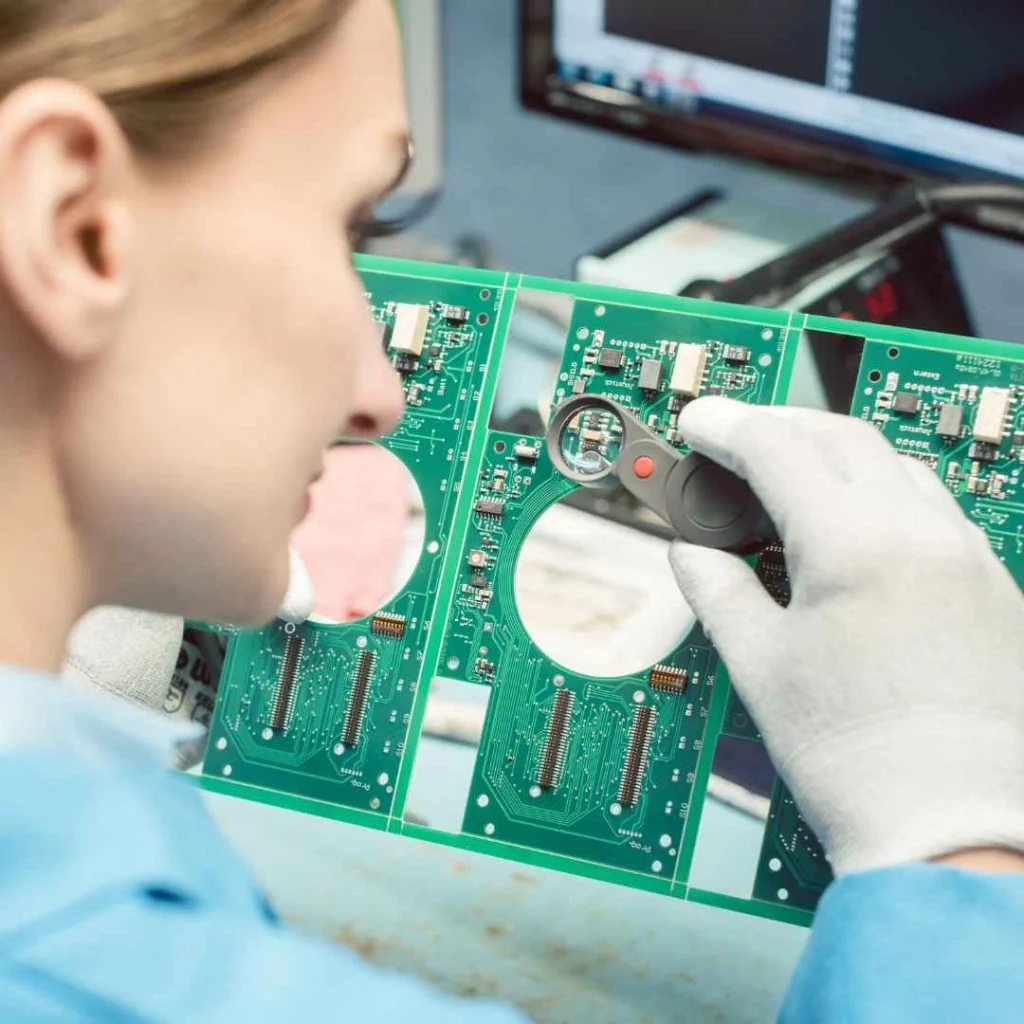
Step 1: Inspect the PCB for Visible Damage
Start by visually inspecting the PCB under good lighting or with a magnifying glass. Look for:
- Dull or discolored copper pads, which indicate oxidation.
- Scratches or uneven coating, suggesting mechanical damage to the OSP layer.
- Residues or smudges that could be contaminants.
If you spot oxidation or contamination, note the affected areas for targeted cleaning or rework.

Step 2: Test Storage and Handling Conditions
Review how the PCB was stored before use. Was it kept in a sealed, dry environment? OSP-finished boards should be stored in vacuum-sealed bags with desiccants to maintain humidity below 30%. If storage conditions were poor, consider this a likely cause of degradation. For future projects, store unused boards at 20-25°C and avoid direct sunlight or humid areas.
Step 3: Clean the PCB Surface
If contamination is suspected, clean the PCB using isopropyl alcohol (at least 90% purity) and a lint-free cloth or brush. Gently wipe the surface to remove oils, dust, or residues. Avoid abrasive materials that could damage the OSP coating further. After cleaning, allow the board to dry completely before soldering.
Step 4: Check Soldering Equipment and Settings
Ensure your soldering iron or reflow oven is set to the correct temperature. For OSP finishes, a soldering temperature of 240-260°C is typically ideal for lead-free solder. Too high a temperature (above 300°C) can burn off the OSP layer, while too low (below 220°C) may result in poor wetting. Also, verify that your solder tip is clean and properly tinned to avoid transferring contaminants to the pad.
Step 5: Use Adequate Flux
Flux is critical for OSP surfaces as it removes minor oxidation and improves wetting. Apply a no-clean or water-soluble flux to the pads before soldering. Be cautious not to overuse flux, as excess residue can cause other issues during assembly. A thin, even layer is sufficient for most DIY repairs.
Step 6: Perform a Test Solder
Solder a single pad or component as a test. Observe if the solder flows evenly and forms a shiny, concave joint. If the solder balls up or refuses to stick, revisit the cleaning and flux application steps. Poor results at this stage may indicate irreversible OSP degradation, requiring more intensive rework.
Step 7: Address Oxidation with Rework Techniques
For oxidized pads where cleaning doesn’t help, gently abrade the surface using a fine-grit fiberglass pen or sandpaper (2000 grit or higher) to expose fresh copper. Be extremely careful not to remove too much material, as this can damage the pad. After abrading, clean the area again with isopropyl alcohol and apply flux before soldering.

Tips for Preventing OSP Solderability Problems
Prevention is always better than rework. Here are practical tips to minimize solder issues with OSP-finished PCBs in your future projects:
- Handle with Care: Always wear gloves when handling OSP PCBs to avoid transferring skin oils. Use tweezers or tools for placement if possible.
- Optimize Storage: Store boards in sealed bags with desiccants in a cool, dry place. Aim for a storage temperature of 20-25°C and humidity below 30%.
- Minimize Heat Cycles: Plan your assembly to avoid multiple reflows. OSP coatings degrade with each heat exposure, so try to complete soldering in one session if possible.
- Use Fresh Boards: Check the manufacturing date of your PCBs. If they’ve been sitting for over 6 months, inspect them closely for degradation before use.
- Choose the Right Flux: Use flux compatible with OSP finishes to ensure proper wetting. Avoid aggressive fluxes that might strip the coating.
When to Seek Professional Help for PCB Rework
While many OSP solderability issues can be resolved with the steps above, some cases may require professional assistance. If you’ve tried cleaning, flux application, and rework techniques but still face poor soldering results across multiple pads, the OSP coating may be irreparably damaged. In such scenarios, consider reaching out to a PCB assembly service for advanced rework or re-coating options. This is especially important for high-value or complex boards where DIY fixes might risk further damage.
Conclusion: Mastering OSP PCB Soldering Challenges
Troubleshooting solderability issues on OSP-finished PCBs doesn’t have to be daunting, even for beginners. By understanding the unique characteristics of OSP coatings, identifying common problems like poor wetting or oxidation, and following a systematic approach to inspection and rework, you can achieve reliable soldering results. Remember to prioritize proper storage, handle boards with care, and use the right tools and techniques to prevent issues from arising in the first place.
Whether you’re working on DIY electronics repair or small-scale production, mastering these skills will save time, reduce frustration, and improve the quality of your projects. Keep experimenting, stay patient, and build your confidence in tackling PCB soldering challenges with OSP finishes.