ALLPCB


If you're new to PCB design and wondering how to improve signal quality in high-speed circuits, backdrilling is a technique worth learning. Simply put, backdrilling, also known as controlled depth drilling, removes unused portions of vias called via stubs to reduce signal interference and enhance performance. In this comprehensive guide, we'll dive deep into what backdrilling is, why it matters for signal quality, and how beginners can understand and apply this process to their PCB designs. Whether you're tackling via stubs or aiming for cleaner signal transmission, this article will walk you through the essentials with practical insights.
What Is Backdrilling in PCB Design?
Backdrilling is a manufacturing technique used in printed circuit board (PCB) production to improve signal integrity, especially in high-speed designs. When a via—a small hole that connects different layers of a PCB—is created, it often extends through the entire board thickness. However, if the signal only needs to travel through part of the via, the unused portion, known as a via stub, can act like an antenna, causing signal reflections and distortions. Backdrilling removes this stub by drilling out the excess copper from the via after the initial plating process, leaving only the necessary conductive path.
For a PCB beginner, think of backdrilling as a way to "clean up" your vias. By eliminating unnecessary copper, you reduce noise and ensure that signals travel smoothly without interference. This technique is particularly crucial in designs operating at high frequencies, where even small imperfections can lead to significant performance issues.
Why Does Signal Quality Matter in PCBs?
Signal quality determines how well data is transmitted across a PCB. In high-speed applications, such as telecommunications or data centers, signals can reach speeds of 10 Gbps or higher. At these rates, any distortion or interference can lead to data errors, slower performance, or complete system failure. Common issues affecting signal quality include crosstalk, noise, and signal reflections, many of which are caused by via stubs in multi-layer boards.
Via stubs are particularly problematic because they create impedance mismatches. For instance, a stub can cause a signal reflection that interferes with the main signal, reducing clarity. Studies suggest that via stubs can increase signal loss by up to 3 dB at frequencies above 5 GHz, which is significant in high-speed designs. Backdrilling addresses this by physically removing the stub, ensuring the signal path is as direct and clean as possible.
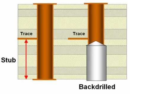
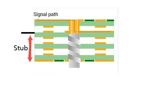
Understanding Via Stubs and Their Impact
Before diving deeper into backdrilling, let’s clarify what via stubs are. In a multi-layer PCB, vias connect traces on different layers. When a via runs through the entire board but the signal only uses a portion of it (say, from layer 2 to layer 4 in a 12-layer board), the unused section below layer 4 becomes a stub. This stub doesn’t carry any useful signal but can still resonate at certain frequencies, causing reflections back into the active signal path.
The longer the stub, the worse the impact. For example, a stub length of just 0.5 mm can create noticeable signal distortion at 10 GHz. This is why controlled depth drilling is essential—it targets and removes these stubs with precision, leaving only the functional part of the via intact.
How Does Backdrilling Work?
Backdrilling is a post-fabrication process that uses specialized drilling equipment to remove the unused copper from a via. Here’s a step-by-step breakdown of how it’s done:
- Initial Via Creation: During PCB fabrication, vias are drilled and plated with copper to connect layers.
- Identification of Stubs: Designers identify which vias have unused portions that need to be removed based on the signal path.
- Controlled Depth Drilling: A numerically controlled (NC) drill targets the via from the opposite side of the board, removing the copper stub to a precise depth. The drill stops just before reaching the active signal layer to avoid damaging the functional part of the via.
- Inspection: The board is inspected to ensure the stub is removed without affecting the rest of the via or nearby components.
The precision of controlled depth drilling is critical. Modern equipment can achieve depth tolerances as tight as ±0.05 mm, ensuring that only the stub is removed. For a PCB beginner, it’s important to note that backdrilling requires careful planning during the design phase to specify which vias need this treatment.
Benefits of Backdrilling for Signal Quality
Backdrilling offers several advantages, especially for high-speed PCB designs. Here are the key benefits:
- Improved Signal Integrity: By eliminating via stubs, backdrilling reduces signal reflections and lowers noise, ensuring cleaner data transmission. This can improve signal integrity by up to 20% in high-frequency applications.
- Reduced Signal Loss: Removing stubs minimizes insertion loss, allowing signals to maintain their strength over longer distances.
- Lower Electromagnetic Interference (EMI): Stubs can act as unintended antennas, emitting or receiving EMI. Backdrilling cuts down on this interference.
- Support for High-Speed Designs: As data rates climb beyond 10 Gbps, backdrilling becomes almost mandatory to meet performance standards in industries like telecommunications and computing.
For beginners, these benefits translate to more reliable designs. Even if you’re not working on cutting-edge technology, understanding backdrilling can help you create boards that perform better and last longer.
When Should You Use Backdrilling?
Backdrilling isn’t necessary for every PCB. It’s most relevant in specific scenarios, such as:
- High-Speed Signals: If your design operates at frequencies above 1 GHz or data rates above 5 Gbps, backdrilling can significantly improve performance.
- Multi-Layer Boards: Boards with 8 or more layers often have longer vias, increasing the likelihood of problematic stubs.
- Critical Applications: Designs for servers, networking equipment, or medical devices where signal quality is non-negotiable often require backdrilling.
If you’re working on simpler, low-speed designs (like a basic LED circuit), backdrilling might be overkill. However, as a PCB beginner, it’s good to recognize when this technique could be useful as your skills and projects advance.
Design Tips for Backdrilling in PCB Layouts
For those new to PCB design, incorporating backdrilling starts with careful planning. Here are some actionable tips to ensure the process goes smoothly:
- Identify Critical Vias Early: During the design phase, mark which vias carry high-speed signals and may need stub removal. This helps the manufacturer know where to apply controlled depth drilling.
- Communicate with Your Manufacturer: Not all fabrication houses offer backdrilling, and those that do may have specific requirements, like minimum via sizes or depth tolerances. Share your design files and discuss your needs upfront.
- Optimize Layer Stackup: Place high-speed signal layers closer to the surface of the board when possible. This reduces stub length and minimizes the need for extensive backdrilling.
- Use Design Software Tools: Many PCB design tools allow you to define backdrill parameters, such as drill depth and via selection, directly in the layout. This ensures accuracy during manufacturing.
Following these steps can save time and prevent costly mistakes. Even as a beginner, paying attention to these details will make your designs more professional and reliable.
Challenges and Limitations of Backdrilling
While backdrilling is a powerful technique, it’s not without challenges. Understanding these can help you decide if it’s the right solution for your project:
- Increased Cost: Backdrilling is an additional manufacturing step, which can raise production costs by 10-20%, depending on the complexity of the board.
- Design Complexity: Specifying backdrill locations requires precision, and errors in planning can lead to damaged vias or signal paths.
- Not Suitable for All Boards: Thin boards or those with very small vias may not be compatible with backdrilling due to equipment limitations.
For a PCB beginner, these challenges highlight the importance of balancing performance needs with budget and design constraints. Always weigh the benefits against the added cost and effort.
Alternatives to Backdrilling for Signal Quality
If backdrilling isn’t feasible for your project, there are other ways to manage via stubs and improve signal quality:
- Blind and Buried Vias: These vias don’t go through the entire board, so they naturally avoid creating stubs. However, they are more expensive to manufacture.
- Via-in-Pad Design: Placing vias directly under component pads can shorten signal paths and reduce stub effects, though this requires careful thermal management.
- Routing Optimization: Adjusting your layer stackup to keep high-speed signals on outer layers can minimize via length and stub impact.
These alternatives can be useful for beginners who are still learning the ropes of PCB design and may not yet need advanced techniques like backdrilling.
Conclusion: Start Enhancing Your PCB Signal Quality with Backdrilling
Backdrilling is a game-changer for anyone looking to boost signal quality in high-speed PCB designs. By removing via stubs through controlled depth drilling, you can eliminate signal reflections, reduce noise, and ensure reliable performance even at data rates exceeding 10 Gbps. For a PCB beginner, understanding backdrilling lays a strong foundation for tackling more complex projects in the future.
Start small by identifying critical vias in your designs and collaborating with your manufacturer to implement this technique where needed. With practice, you’ll gain confidence in using backdrilling to create cleaner, more efficient boards. Remember, signal quality isn’t just a technical detail—it’s the key to building reliable electronics that meet today’s demanding standards.