ALLPCB


Designing a printed circuit board (PCB) is a delicate balancing act, especially when it comes to copper thickness (measured in mils) and trace width. These two factors play a critical role in determining a PCB’s current carrying capacity, impedance control, and signal integrity. So, how do you strike the right balance for optimal performance? In short, it involves understanding the relationship between copper weight, trace width, and your design requirements, then applying industry standards and calculations to meet electrical and thermal needs.
In this comprehensive guide, we’ll dive deep into the essentials of PCB trace design, exploring how copper weight vs trace width impacts performance. Whether you’re an engineer working on high-power circuits or high-speed digital designs, this blog will provide actionable insights to help you achieve reliable and efficient PCB layouts. Let’s explore the key considerations for current carrying capacity, impedance control, and signal integrity to ensure your designs perform at their best.
Why Copper Thickness and Trace Width Matter in PCB Design
When designing a PCB, every element must work together to ensure functionality, reliability, and efficiency. Copper thickness, often referred to as copper weight (measured in ounces per square foot or mils), and trace width directly influence how much current a trace can carry, how well it maintains signal integrity, and how it manages heat. A mismatch in these parameters can lead to overheating, signal distortion, or even board failure.
Copper thickness typically ranges from 0.5 oz (0.7 mils) to 2 oz (2.8 mils) for standard designs, though heavier weights like 3 oz or more are used for high-power applications. Trace width, on the other hand, is the physical width of the copper path on the board, often measured in mils (thousandths of an inch). Balancing these two aspects is crucial for meeting the electrical and mechanical demands of your circuit.
Understanding Copper Weight vs Trace Width in PCB Trace Design
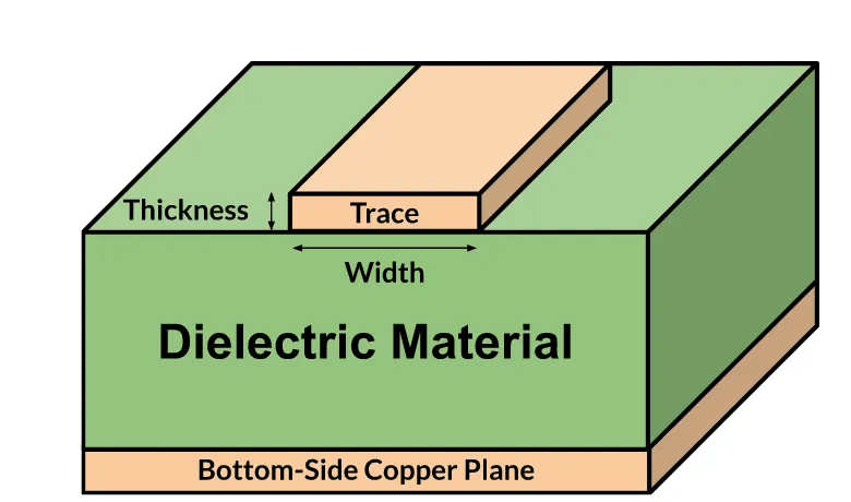
The relationship between copper weight and trace width is foundational to PCB performance. Copper weight determines the thickness of the copper layer on the board, while trace width defines how wide the conductive path is. Together, they determine the cross-sectional area of the trace, which directly impacts its ability to handle current and resist heat buildup.
For instance, a 1 oz copper layer (1.4 mils thick) with a trace width of 10 mils has a much smaller cross-sectional area than the same copper weight with a 50 mil trace width. The larger area can carry more current with less resistance, reducing the risk of overheating. However, wider traces take up more board space, which can be a constraint in compact designs.
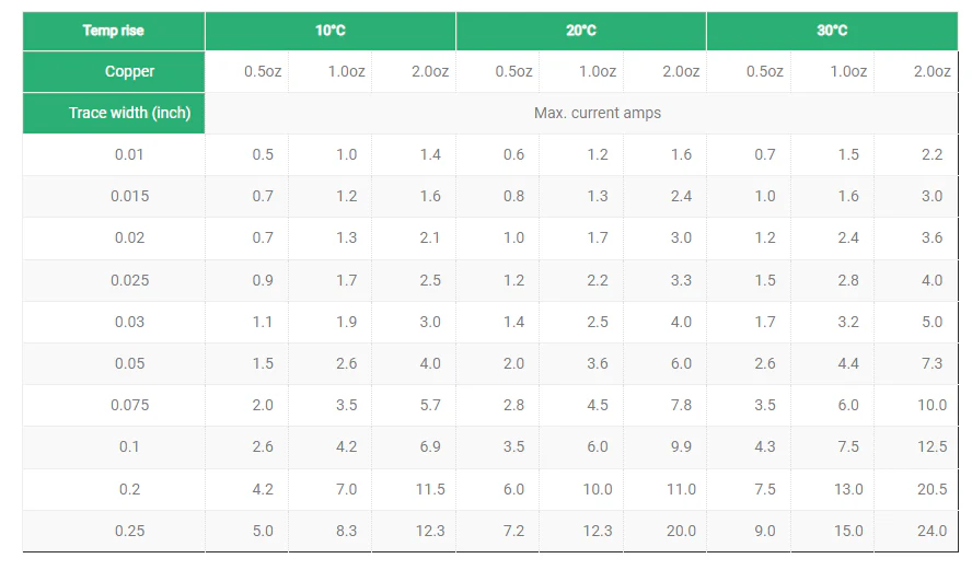
Standard industry guidelines, such as those from the Institute of Printed Circuits (IPC), suggest that for a 1 oz copper weight, a 10 mil trace can handle approximately 1 amp of current with a temperature rise of 10°C. For higher currents, you’ll need either wider traces or thicker copper. This balance is critical in high-power designs where thermal management is a priority.
Current Carrying Capacity: How Much Can Your Trace Handle?
Current carrying capacity is one of the most important factors in PCB trace design. It refers to the maximum amount of current a trace can handle without exceeding a safe temperature rise. If a trace is too narrow or the copper too thin for the current load, it can overheat, leading to performance issues or even permanent damage.
The current carrying capacity depends on the cross-sectional area of the trace (width multiplied by thickness) and the acceptable temperature rise. According to IPC-2221 standards, a trace with 1 oz copper and a width of 20 mils can carry around 1.5 amps with a 10°C temperature increase. For a 2 oz copper layer, the same width can handle roughly double the current, or 3 amps, under similar conditions.
To calculate the required trace width for a specific current, you can use online tools or formulas based on IPC standards. For example, if your circuit needs to carry 5 amps with a 1 oz copper layer and a maximum temperature rise of 20°C, you might need a trace width of approximately 100 mils. Adjusting copper thickness to 2 oz could reduce this width to around 50 mils, saving valuable board space.
Impedance Control: Ensuring Signal Quality in High-Speed Designs
In high-speed digital circuits, impedance control becomes a critical aspect of PCB trace design. Impedance, measured in ohms, is the resistance to the flow of alternating current (AC) signals and is influenced by trace width, copper thickness, dielectric material, and trace spacing. Mismatched impedance can cause signal reflections, leading to data errors or degraded performance.
For controlled impedance designs, such as those used in USB, HDMI, or RF applications, trace width and copper thickness must be carefully calculated to match the target impedance, often 50 ohms or 100 ohms for differential pairs. Thicker copper can reduce resistance, but it also affects the characteristic impedance by altering the relationship between the trace and the ground plane. Similarly, wider traces lower impedance, while narrower traces increase it.
As an example, for a 50-ohm single-ended trace on a standard FR-4 substrate with a 1 oz copper layer, a trace width of around 6 mils might be needed if the dielectric thickness is 5 mils. If you switch to a 2 oz copper layer, the trace width may need slight adjustment to maintain the same impedance due to changes in the effective dielectric constant.
Using simulation tools or impedance calculators during the design phase can help fine-tune these parameters. Proper impedance control ensures that signals travel without distortion, maintaining the integrity of high-speed data transmission.
Signal Integrity: Minimizing Noise and Interference
Signal integrity refers to the quality of an electrical signal as it travels through a PCB. Poor signal integrity can result in noise, crosstalk, or data loss, especially in high-frequency or high-speed applications. Copper thickness and trace width both play roles in maintaining signal integrity, alongside other factors like trace length and routing.
Thicker copper layers can reduce resistive losses, which is beneficial for maintaining signal strength over long traces. However, they can also increase parasitic capacitance if not paired with appropriate dielectric spacing, potentially leading to signal delays or distortion. Wider traces can help lower resistance and improve current flow, but they may introduce more crosstalk if placed too close to neighboring traces.
For example, in a design operating at 1 GHz, minimizing signal loss is critical. Using a 1.5 oz copper layer instead of 1 oz can reduce resistive losses by nearly 30%, improving signal quality. At the same time, ensuring proper trace spacing (often at least 3 times the trace width for high-speed signals) helps minimize interference between adjacent lines.
Balancing copper thickness and trace width with careful routing practices is essential for preserving signal integrity. Layer stack-up design, ground planes, and via placement also contribute significantly to this aspect of PCB performance.
Finding the Optimal Balance: Practical Tips for PCB Designers
Balancing copper thickness and trace width is both an art and a science. Here are some practical tips to guide you through the process:
- Start with Requirements: Define the electrical needs of your design, including current load, operating frequency, and impedance targets. Use these as the foundation for selecting copper weight and trace width.
- Use Industry Standards: Refer to IPC-2221 or IPC-2152 guidelines for current carrying capacity and thermal management. These standards provide reliable data for safe trace sizing.
- Leverage Design Tools: Utilize PCB design software with built-in calculators for trace width, impedance, and thermal analysis. These tools can save time and reduce errors.
- Consider Manufacturing Constraints: Thicker copper layers and very narrow traces can increase production costs or complexity. Check with your fabrication partner to ensure your design is manufacturable.
- Test and Iterate: Simulate your design to identify potential issues with signal integrity or heat dissipation. Make adjustments as needed before finalizing the layout.
Common Challenges and How to Overcome Them
Designing with copper thickness and trace width in mind often comes with challenges. Here are a few common issues and solutions:
Space Limitations: In compact designs, wider traces may not fit. Consider increasing copper thickness to handle higher currents without widening traces, or use multiple layers to distribute current.
Thermal Management: High-current traces can generate heat. Add thermal vias, heat sinks, or increase copper weight to dissipate heat effectively.
Cost Constraints: Thicker copper layers are more expensive. Optimize your design by using heavier copper only where necessary, such as on power traces, while keeping signal traces at standard thickness.
Signal Integrity Issues: High-speed signals can suffer from crosstalk or reflections. Maintain consistent trace width, use ground planes, and follow impedance matching guidelines to minimize these effects.
The Impact of Copper Thickness and Trace Width on Manufacturing
The choices you make in copper thickness and trace width don’t just affect performance—they also influence the manufacturing process. Thicker copper layers require more etching time and can lead to undercutting, where the trace edges become uneven, potentially affecting impedance. Narrow traces with heavy copper can also be prone to defects if the fabrication process isn’t tightly controlled.
Standard copper weights like 1 oz are widely supported and cost-effective for most applications. If your design calls for 2 oz or higher, communicate early with your manufacturing partner to confirm capabilities and discuss any design adjustments needed for reliability.
Conclusion: Mastering the Balance for PCB Success
Balancing copper thickness (mils) and trace width is a cornerstone of effective PCB trace design. By carefully considering current carrying capacity, impedance control, and signal integrity, you can create boards that perform reliably under a wide range of conditions. Whether you’re designing for high-power applications or high-speed digital circuits, the principles of copper weight vs trace width remain the same: understand your requirements, apply industry standards, and use the right tools to fine-tune your design.
With the insights and tips provided in this guide, you’re well-equipped to tackle the challenges of PCB design and achieve optimal performance. Remember that every design is unique, so take the time to analyze, simulate, and refine your approach. A well-balanced PCB not only meets technical specifications but also ensures long-term durability and efficiency.