 ALLPCB


Introduction
In PCB assembly, the solder paste printing step sets the foundation for reliable component placement and soldering. Stencils act as precision templates, depositing exact volumes of solder paste onto pads before components arrive. Choosing the right stencil material directly influences print quality, yield rates, and long-term process stability. Engineers often face decisions between durability, precision, and cost when specifying stainless steel versus nickel options. Factors like pitch size, volume production, and defect troubleshooting guide these choices. This article explores material comparisons, thickness guidelines, and enhancements to optimize your SMT process.
Understanding SMT Stencils and Their Role in Assembly
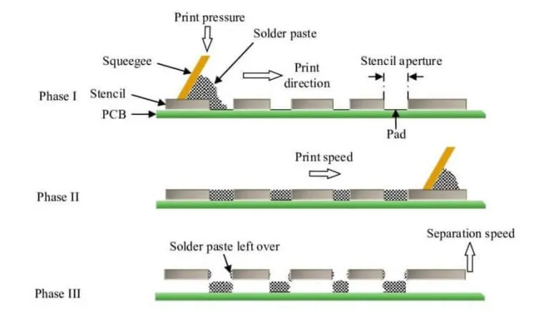
SMT stencils consist of thin metal foils with laser-cut or electroformed apertures matching pad layouts. During printing, a squeegee blade pushes solder paste through these openings, forming uniform deposits. Poor stencil performance leads to defects such as bridging, insufficient paste, or tombstoning in reflow. Material selection affects aperture wall smoothness, paste release, and resistance to wear over thousands of prints. In high-density boards with fine-pitch components, even minor variations in stencil properties can cascade into assembly failures. Engineers must balance these attributes against production demands for consistent results.
Standards like IPC-7525C provide guidelines for aperture design and material considerations to ensure repeatability. Stainless steel dominates general applications due to its availability and robustness. Nickel variants offer advantages in specialized scenarios. Process engineers troubleshoot by inspecting aperture fidelity and paste transfer efficiency after initial runs. Selecting the optimal stencil prevents downtime and rework in volume manufacturing.
Stainless Steel vs Nickel Stencil: A Detailed Comparison
Stainless steel stencils represent the workhorse of PCB assembly, offering excellent mechanical strength and corrosion resistance for everyday use. These laser-cut foils handle high squeegee pressures without deforming, making them ideal for prototypes and medium-volume runs. Their etched or trapezoidal apertures provide good paste release in standard pitches above 0.5 mm. However, stainless steel surfaces exhibit higher roughness compared to alternatives, potentially leading to paste residue buildup over time. Engineers appreciate their cost-effectiveness, as they withstand 50,000 or more prints before significant wear.
Nickel stencils, often electroformed, deliver superior precision for fine-pitch applications like 0.3 mm or smaller components. The electroforming process creates smoother, harder aperture walls with minimal burrs, improving solder paste transfer efficiency. This reduces bridging risks and enhances release, especially with Type 4 or finer paste powders. Nickel options excel in high-reliability sectors where ultra-fine features demand tight tolerances. Drawbacks include higher upfront costs and potential brittleness under extreme pressures. Troubleshooting tip: if stainless steel prints show inconsistent deposits on small pads, switch to nickel for better wall quality.
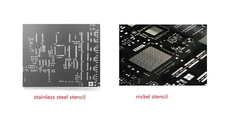
In stainless steel vs nickel stencil debates, production volume tips the scale toward steel for cost savings, while precision needs favor nickel. Both materials comply with IPC guidelines for aperture aspect ratios above 1.5 and area ratios exceeding 0.66. Test prints reveal nickel's edge in transfer efficiency for low-area-ratio apertures. Maintenance differs too: steel requires more frequent underside wiping, while nickel's inherent smoothness extends clean cycles. Engineers should profile paste rheology alongside material choice for optimal results.
Stencil Thickness Selection Guide
Stencil thickness controls solder paste volume, directly impacting joint fillet formation after reflow. Thicker stencils deposit more paste, suiting larger components like QFPs or connectors with pitches over 0.65 mm. Common thicknesses range from 0.100 mm to 0.150 mm, selected based on smallest aperture dimensions. For fine-pitch BGAs or 01005 passives, thinner foils around 0.076 mm to 0.100 mm prevent bridging while ensuring adequate standoff. IPC-7525C outlines rules tying thickness to pad size, recommending calculations for volume consistency across the board.
Start with aperture width-to-thickness ratios; aim for at least 1:1 to avoid paste starvation. For mixed-technology boards, hybrid thinning, lasers thin select areas for fine features while keeping bulk thickness standard. Engineers troubleshoot thickness issues by measuring deposit heights post-print and adjusting for paste type. Too thick a stencil causes bridging on tight pitches; too thin leads to head-in-pillow defects. Validate choices with SPI data, targeting 75-125% transfer efficiency.
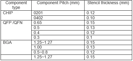
A practical stencil thickness selection guide involves component audits: 0.125 mm serves most 0.5 mm pitch assemblies, dropping to 0.100 mm for 0.4 mm or below. Factor in board warpage and printer setup for flatness. Post-reflow inspections confirm fillet adequacy per J-STD-001 requirements. Iterative testing refines selections, especially when scaling from prototype to production.
Stencil Nano Coating Benefits
Nano coatings apply a thin, oleophobic layer to stencil undersides and aperture edges, revolutionizing paste release. These treatments repel solder paste residues, minimizing adhesion and bridging on high-density boards. Benefits include extended print-to-clean cycles, often doubling intervals between wipes for sustained efficiency. In fine-pitch printing, nano coatings boost transfer rates by 5-10% on small apertures, reducing defects like insufficient solder. Maintenance simplifies, as residues wipe off easily without solvents.
Engineers report fewer bridging incidents and higher first-pass yields with coated stencils. The coating withstands abrasion from squeegee passes, maintaining performance over 100,000 prints. Pairing nano coatings with nickel amplifies smoothness gains. Troubleshooting sticky paste? Apply coatings to stainless steel for quick improvements without material swaps. Durability varies by formulation, but quality options resist reflow temperatures up to 260°C.
Stencil nano coating benefits extend to process stability, especially with lead-free pastes prone to slumping. They lower total cost of ownership by cutting cleaning time and paste waste. Validate via high-speed imaging of print releases. For ultra-fine pitch, coatings prevent powder clogging in Type 5 pastes.
Best Practices for Stencil Selection and Use
Align stencil specs with land patterns from IPC-7351 libraries for volume matching. Specify frameless or framed based on printer fixturing; frameless suits flexibility. Etch orientation matters: downward-facing trapezoids aid release on stainless steel. Store stencils flat in clean environments to prevent warping. Pre-print inspections check aperture integrity with optical comparators.
During production, monitor squeegee speed and pressure; 20-50 mm/s works for most setups. Use stainless steel for pitches >0.5 mm, nickel below. Apply nano coatings universally for yields above 99%. Troubleshoot bridging by reducing thickness or adding coatings first
Clean ultrasonically weekly, avoiding harsh abrasives. Track print counts to predict wear. For mixed assemblies, segment stencils by zone thickness.
Troubleshooting Common Stencil-Related Issues
Insufficient paste often traces to thick stencils or poor release; thin down or coat apertures. Bridging plagues fine pitches: optimize thickness per guide, ensure area ratios exceed 0.66. Smeared deposits signal dirty undersides; nano coatings cut this dramatically. Warped stencils cause uneven prints; tension properly in the frame.
Aperture clogging hits with fine powders: select Type 4+ paste, clean frequently. Test electroformed nickel for stubborn ultra-fine features. SPI data pinpoints issues early. Adjust gasketing for board-stencil gaps under 50 μm.
Conclusion
Selecting stencil materials hinges on balancing precision, durability, and cost for your PCB assembly needs. Stainless steel suits robust, economical runs, while nickel excels in fine-pitch challenges. Follow a stencil thickness selection guide tied to IPC-7525C for volume control. Embrace stencil nano coating benefits to slash defects and maintenance. Practical troubleshooting ensures peak performance. Optimize these elements for reliable, high-yield SMT processes.
FAQs
Q1: What are the key differences in stainless steel vs nickel stencil performance?
A1: Stainless steel stencils provide durable, cost-effective options for standard pitches and high-volume printing, handling wear well. Nickel stencils offer smoother apertures and better paste release for fine-pitch components under 0.4 mm, reducing bridging. Choose steel for prototypes, nickel for precision. Test transfer efficiency to confirm fit.
Q2: How does stencil nano coating benefits improve PCB assembly yields?
A2: Stencil nano coating benefits include superior paste release, fewer clean cycles, and lower defect rates like bridging on dense boards. Coatings on apertures and undersides repel residues, boosting efficiency for Type 5 pastes. Yields rise with consistent deposits. Ideal for high-mix lines.
Q3: What is a reliable stencil thickness selection guide for fine-pitch SMT?
A3: A stencil thickness selection guide recommends 0.100-0.125 mm for 0.5 mm pitches, thinning to 0.076 mm for 0.3 mm or smaller. Match to aperture size per IPC rules, ensuring ratios support paste volume. SPI validates post-print. Adjust for component standoff.
Q4: When should I choose nickel over stainless steel stencils?
A4: Opt for nickel stencils in stainless steel vs nickel stencil scenarios demanding ultra-smooth walls, like 01005 components or high-reliability apps. They minimize residue and improve release. Use stainless for coarser pitches to save costs. Profile your process first.


