 ALLPCB


When designing high-density interconnect (HDI) printed circuit boards (PCBs), choosing between stacked and staggered blind and buried vias is a critical decision that impacts performance, reliability, and manufacturability. So, what’s the difference, and which should you choose? In short, stacked vias are vertically aligned connections between layers, ideal for saving space in compact designs, while staggered vias are offset, offering better reliability and thermal management. This blog dives deep into the design considerations for both, focusing on via reliability, HDI PCB routing, and via design rules to help you make informed decisions for your next project.
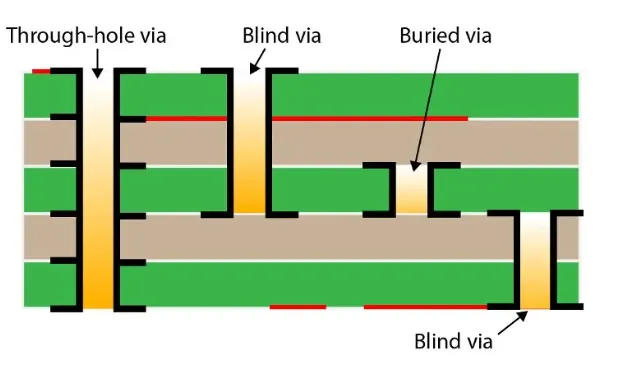
What Are Blind and Buried Vias in HDI PCBs?
Before we compare stacked and staggered vias, let’s clarify what blind and buried vias are. Blind vias connect an outer layer of a PCB to an inner layer but do not go through the entire board. Buried vias, on the other hand, connect inner layers only and are not visible from the surface. Both are essential in HDI PCB designs where space is limited, and signal integrity is crucial. These vias enable denser layouts by reducing the need for through-hole vias that take up valuable space across all layers.
In HDI designs, blind and buried vias are often arranged in either a stacked or staggered configuration, depending on the project’s needs. Understanding their differences is key to optimizing your PCB for performance and cost.
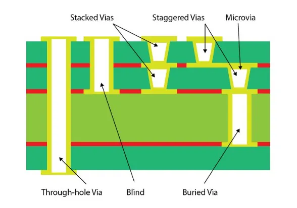
Stacked Vias: Definition and Key Features
Stacked vias are a series of blind or buried vias placed directly on top of each other to connect multiple layers in a vertical alignment. This configuration is common in HDI PCBs where board real estate is at a premium, as it minimizes the horizontal space needed for interconnections.
Key Features of Stacked Vias:
- Space Efficiency: By stacking vias vertically, you can achieve higher density in a smaller footprint, ideal for compact devices like smartphones or wearable tech.
- Signal Integrity: Stacked vias provide a shorter signal path, which can reduce impedance and signal delay. For high-speed signals (e.g., above 5 GHz), this can be a significant advantage.
- Complex Manufacturing: Stacking vias requires precise drilling and plating processes, often involving laser drilling for microvias (diameters as small as 0.1 mm). This can increase production costs.
Stacked vias are often used in applications requiring tight routing, such as in advanced medical devices or high-performance computing hardware. However, their design must follow strict via design rules to avoid reliability issues, which we’ll cover later.
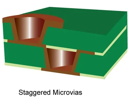
Staggered Vias: Definition and Key Features
Staggered vias, in contrast, are offset from each other rather than aligned vertically. Instead of stacking directly on top, each via is placed at a slight horizontal distance, creating a zigzag pattern when viewed in a cross-section of the PCB.
Key Features of Staggered Vias:
- Improved Reliability: The offset design reduces stress concentration during thermal cycling, lowering the risk of via cracking or delamination. This is critical for boards exposed to temperature fluctuations (e.g., -40°C to 85°C in automotive applications).
- Better Thermal Management: Staggered vias distribute heat more evenly across the board, preventing hotspots that can degrade performance.
- Easier Manufacturing: The offset placement is less demanding on drilling precision, often resulting in lower production costs compared to stacked vias.
Staggered vias are preferred in applications where reliability and thermal performance outweigh the need for extreme density, such as in industrial control systems or automotive electronics.
Design Considerations for Stacked Vias
Designing with stacked vias requires careful planning to balance their space-saving benefits with potential challenges. Here are the key considerations:
1. Via Reliability
Stacked vias, especially microvias with aspect ratios (depth-to-diameter) greater than 1:1, are prone to reliability issues like cracking or incomplete plating. For example, a microvia with a 0.1 mm diameter and 0.15 mm depth has an aspect ratio of 1.5:1, pushing the limits of standard manufacturing. To improve reliability, ensure that plating thickness meets at least 20-25 micrometers, as per IPC-6012 standards for Class 3 products.
2. HDI PCB Routing Challenges
In HDI PCB routing, stacked vias allow for tighter trace layouts, often supporting trace widths as narrow as 0.075 mm. However, their vertical alignment can create signal crosstalk if high-speed traces (e.g., 10 Gbps signals) are routed nearby without proper shielding or ground planes. Use simulation tools to check for impedance mismatches, targeting a characteristic impedance of 50 ohms for most high-speed designs.
3. Manufacturing Constraints
Stacked vias often require sequential lamination, where layers are built and drilled in stages. This process increases fabrication time and cost, especially for boards with more than two stacked microvias. Check with your manufacturer for their capability limits—some may restrict stacking to two levels for vias smaller than 0.15 mm in diameter.
Design Considerations for Staggered Vias
Staggered vias offer different advantages and challenges. Here’s what to keep in mind when incorporating them into your design:
1. Via Reliability
Staggered vias are inherently more reliable due to reduced mechanical stress. Studies show that staggered configurations can withstand up to 30% more thermal cycles before failure compared to stacked vias, making them suitable for harsh environments. Ensure proper spacing (at least 0.2 mm between via centers) to avoid overlapping stress zones.
2. HDI PCB Routing Flexibility
While staggered vias take up more horizontal space, they offer greater flexibility in routing. The offset design allows for easier placement of traces between vias, reducing the risk of signal interference. For differential pairs operating at 1-2 GHz, staggered vias can help maintain signal integrity by providing more room for controlled impedance routing.
3. Cost and Manufacturability
Staggered vias are generally easier and cheaper to manufacture since they don’t require the precision of vertical alignment. This can reduce drilling costs by up to 15-20% compared to stacked vias, depending on the board complexity and layer count. However, the larger footprint may limit their use in ultra-compact designs.
Via Design Rules for Stacked and Staggered Vias
Regardless of whether you choose stacked or staggered vias, adhering to via design rules is essential for a successful HDI PCB design. Here are some universal guidelines:
- Aspect Ratio: Keep the via aspect ratio below 1:1 for microvias to ensure proper plating and reliability. For standard blind vias, aim for ratios under 10:1.
- Pad Size: Ensure via pads are at least 0.1-0.15 mm larger than the via diameter to provide a stable connection and prevent breakout during drilling.
- Spacing: Maintain a minimum spacing of 0.2 mm between vias to avoid electrical shorts or manufacturing defects. For staggered vias, this spacing also helps with thermal distribution.
- Layer Transitions: Limit stacked vias to 1-2 layer transitions for microvias to minimize reliability risks. For deeper connections, consider using buried vias with staggered placement.
- Material Selection: Use high-Tg (glass transition temperature) materials (e.g., FR-4 with Tg of 170°C) for boards with stacked vias to handle thermal stress during reflow soldering.
Following these rules helps ensure that your vias—whether stacked or staggered—perform reliably under operational conditions.
Stacked vs. Staggered Vias: Which Should You Choose?
Deciding between stacked and staggered vias depends on your project’s specific requirements. Here’s a breakdown to guide your choice:
- Choose Stacked Vias If: Your design prioritizes space savings and high-density routing. They’re ideal for compact, high-speed applications where signal paths need to be as short as possible, such as in 5G modules or advanced consumer electronics.
- Choose Staggered Vias If: Reliability and thermal performance are your top concerns. They’re better suited for applications in harsh environments, like automotive or industrial systems, where the board must endure temperature swings and mechanical stress.
For many designs, a hybrid approach—using both stacked and staggered vias in different areas of the board—can provide the best of both worlds. For instance, use stacked vias in high-density areas near ICs and staggered vias in power delivery sections to improve heat dissipation.
Impact on Signal Integrity and Performance
Signal integrity is a major concern in HDI PCB routing, and via configuration plays a big role. Stacked vias, with their shorter vertical paths, typically introduce less parasitic inductance—often below 0.5 nH per via—making them better for high-frequency signals above 5 GHz. However, if not properly shielded, they can cause crosstalk due to their close proximity in dense layouts.
Staggered vias, while slightly increasing inductance (up to 0.8 nH per via), reduce crosstalk by spreading out connections. They’re often a safer choice for mixed-signal designs where analog and digital signals share the same board. To optimize performance, pair both configurations with solid ground planes and maintain a 50-ohm impedance for critical traces.
Cost Implications of Stacked vs. Staggered Vias
Cost is always a factor in PCB design. Stacked vias, due to their complex manufacturing process, can increase fabrication costs by 20-30% compared to staggered vias, especially for boards with multiple stacked microvias. This cost rises further if sequential lamination or advanced laser drilling is required.
Staggered vias, being easier to drill and plate, keep production costs lower. They also reduce the risk of manufacturing defects, which can save money on rework or scrap. For budget-conscious projects, staggered vias are often the more economical choice unless density requirements demand stacked vias.
Conclusion: Balancing Design Needs with Practicality
Both stacked and staggered blind and buried vias have their place in HDI PCB design. Stacked vias excel in ultra-compact, high-speed applications where space is critical, while staggered vias offer superior reliability and thermal management for demanding environments. By understanding the design considerations—via reliability, HDI PCB routing challenges, and via design rules—you can select the right configuration for your project.
Ultimately, the best choice depends on balancing performance needs with manufacturing constraints and cost. Whether you opt for stacked vias to maximize density or staggered vias for durability, following best practices and collaborating closely with your PCB manufacturer will ensure a successful design. With the right approach, you can achieve a high-performing, reliable board tailored to your application’s unique demands.


