 ALLPCB


When it comes to PCB design, one key decision is whether to use single-sided silkscreen or double-sided silkscreen printing. If you're wondering which is right for your project, here's the quick answer: single-sided silkscreen is ideal for simpler, cost-effective designs with components on one side, while double-sided silkscreen suits complex, high-density boards with components on both sides, offering better labeling and assembly guidance. In this in-depth guide, we'll break down the differences, benefits, and PCB design considerations for each option to help you make an informed choice for your next project.
What is PCB Silkscreen and Why Does It Matter?
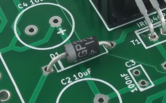
Before diving into the comparison of single-sided silkscreen and double-sided silkscreen, let's clarify what a silkscreen layer is. The silkscreen is a printed layer on a printed circuit board (PCB) that includes text, symbols, and markings. These markings help identify components, indicate polarity, label test points, and provide assembly instructions. Typically made from a non-conductive epoxy ink, the silkscreen layer is crucial for manufacturing, testing, and maintenance of electronic devices.
Choosing between single-sided and double-sided silkscreen printing impacts not only the cost and complexity of your PCB but also its usability and assembly efficiency. Whether you're designing a simple consumer gadget or a high-tech industrial system, understanding PCB silkscreen requirements is essential for a successful outcome.
Single-Sided Silkscreen: The Basics and Benefits
Single-sided silkscreen refers to printing the silkscreen layer on only one side of the PCB, typically the side where components are mounted. This is the most common and cost-effective option for many designs, especially for simpler circuits.
Key Features of Single-Sided Silkscreen
- One-Sided Printing: Markings are applied only on the top or bottom layer, depending on component placement.
- Lower Cost: Since printing is done on just one side, manufacturing expenses are reduced.
- Simpler Design: Best for boards with components on a single side, reducing the need for dual-side labeling.
Advantages of Single-Sided Silkscreen
Single-sided silkscreen is a go-to choice for many engineers due to its simplicity and affordability. Here are some specific benefits:
- Cost-Effective for Low-Complexity Projects: If your PCB design is straightforward—say, for a basic LED circuit or a small sensor module—single-sided silkscreen keeps production costs down. For instance, a typical single-sided silkscreen process can save up to 15-20% in printing costs compared to double-sided options.
- Faster Production: With printing limited to one side, the manufacturing process is quicker, which is ideal for rapid prototyping or small-batch runs.
- Sufficient for Many Applications: Many consumer electronics, such as calculators or remote controls, use single-sided silkscreen since components are often mounted on one side only.
Limitations of Single-Sided Silkscreen
While single-sided silkscreen is practical for basic designs, it may fall short for more advanced projects:
- Limited Labeling Space: If your board has components on both sides, single-sided printing means the unprinted side lacks markings, which can complicate assembly and debugging.
- Not Ideal for High-Density Designs: Complex boards with dual-side component placement often require markings on both sides for clarity.
Double-Sided Silkscreen: When Complexity Calls
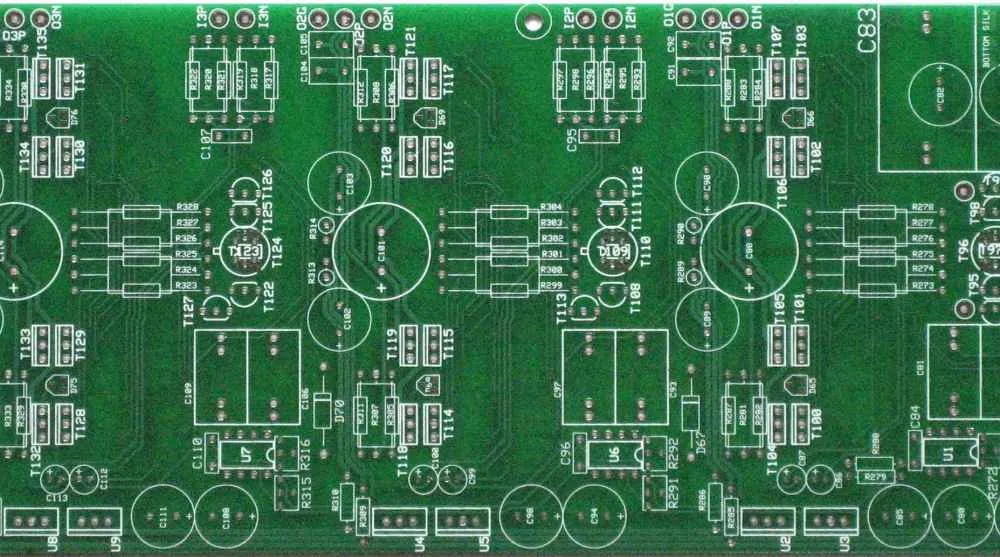
Double-sided silkscreen involves printing markings on both the top and bottom layers of the PCB. This option is tailored for more intricate designs where components are placed on both sides of the board.
Key Features of Double-Sided Silkscreen
- Dual-Side Printing: Markings are applied to both surfaces of the PCB, providing comprehensive labeling.
- Higher Cost: The additional printing process increases manufacturing expenses.
- Enhanced Clarity: Ideal for boards with components on both sides, ensuring all parts are clearly labeled.
Advantages of Double-Sided Silkscreen
For complex projects, double-sided silkscreen offers distinct advantages that can outweigh the added cost:
- Better Assembly Guidance: With markings on both sides, assemblers can easily identify component placements and orientations, reducing errors. This is critical for high-density designs, such as those in smartphones or industrial control systems, where components might number in the hundreds.
- Improved Debugging and Maintenance: Technicians can refer to silkscreen markings on both sides during testing or repairs, speeding up troubleshooting. For example, a double-sided silkscreen can clearly indicate test points on both layers, cutting diagnostic time by up to 30% in some cases.
- Supports Advanced Designs: Modern electronics often require dual-side component mounting to save space. Double-sided silkscreen ensures that every part, whether on the top or bottom, is properly documented.
Limitations of Double-Sided Silkscreen
Despite its benefits, double-sided silkscreen isn't always the best fit:
- Higher Cost: The dual printing process can increase costs by 20-30% compared to single-sided options, which might not be justified for simpler designs.
- Longer Production Time: Printing on both sides adds a step to the manufacturing process, potentially delaying delivery for time-sensitive projects.
PCB Design Considerations for Silkscreen Layers
Whether you choose single-sided or double-sided silkscreen, certain PCB design considerations apply to ensure the silkscreen layer is effective and functional. These guidelines help optimize readability, assembly accuracy, and manufacturing efficiency.
Font Size and Line Width
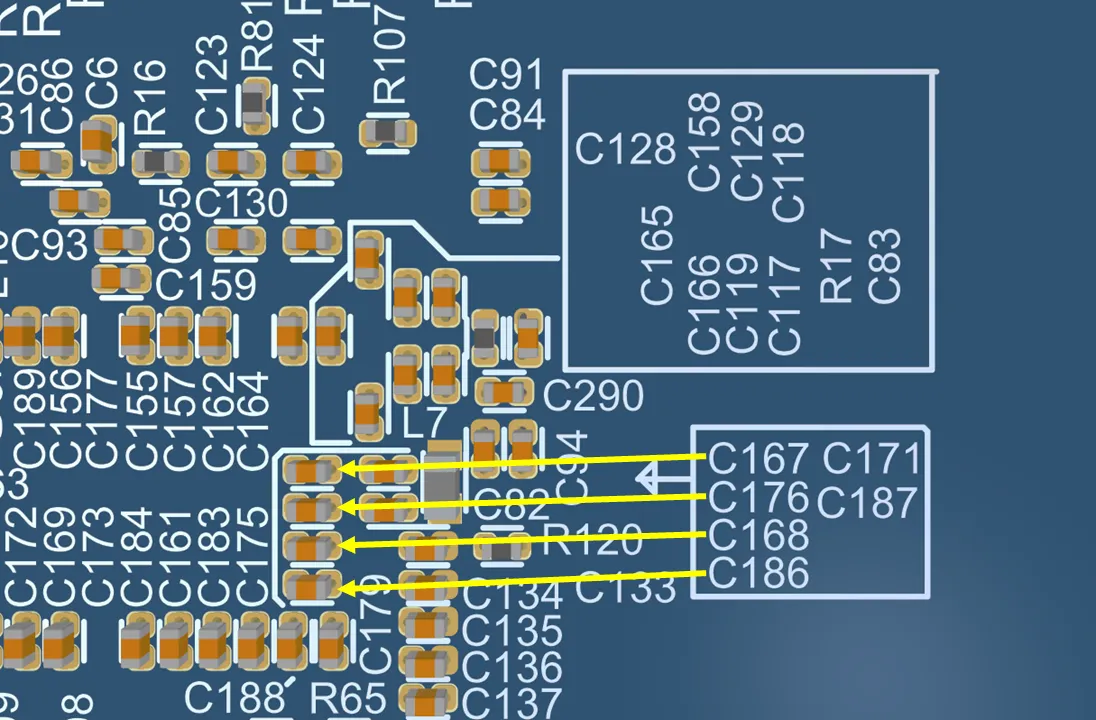
The silkscreen text and symbols must be legible to the naked eye. Industry standards recommend a minimum line width of 5 mils (0.005 inches) and a character height of at least 50 mils (0.05 inches). Smaller sizes can lead to unclear markings, causing assembly errors.
Placement and Spacing
Ensure silkscreen markings do not overlap with solder pads or vias, as this can interfere with soldering or component placement. Maintain a spacing of at least 10 mils between silkscreen elements to prevent smudging during printing.
Orientation for Readability
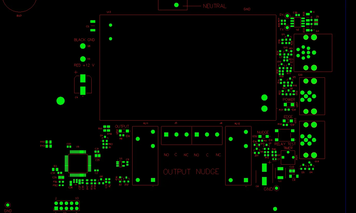
All text and symbols should follow a uniform reading direction, typically left-to-right and top-to-bottom. This consistency helps assemblers and technicians quickly interpret the markings without confusion.
Color Contrast
Silkscreen ink, often white or black, should contrast with the PCB's solder mask color (commonly green, blue, or red). For instance, white ink on a green mask provides high visibility, while black ink might be better on lighter masks for readability.
Avoiding Impedance Issues
While silkscreen ink is non-conductive, improper placement near high-speed signal traces could theoretically affect impedance. For critical designs, such as those with signal speeds above 1 GHz, keep silkscreen markings away from sensitive areas to maintain signal integrity (typical impedance targets for high-speed designs are around 50 ohms for single-ended traces).
PCB Silkscreen Requirements: Single vs. Double-Sided
Understanding the specific PCB silkscreen requirements for single-sided and double-sided printing can help streamline your design process and avoid manufacturing hiccups. Here's a breakdown of what to keep in mind for each.
Single-Sided Silkscreen Requirements
- Focus on One Layer: Ensure all necessary markings—component identifiers, polarity indicators, and test points—are included on the chosen side. There’s no second side to fall back on, so completeness is key.
- Maximize Space Efficiency: With limited real estate, prioritize critical information and avoid clutter. For example, use abbreviations for component labels if space is tight (e.g., "R1" for resistor 1).
- Check Component Placement: Confirm that the silkscreen side matches the component mounting side to avoid confusion during assembly.
Double-Sided Silkscreen Requirements
- Consistency Across Layers: Ensure markings on both sides follow the same style and formatting for a cohesive look. For instance, if polarity markers on the top layer use a "+" symbol, use the same on the bottom.
- Account for Dual Printing Costs: Budget for the additional printing expense and verify with your manufacturer that their process supports double-sided silkscreen with high precision.
- Balance Information: Distribute markings logically between the top and bottom layers based on component placement, avoiding overloading one side with text while the other remains sparse.
Which is Right for Your Project?
Choosing between single-sided silkscreen and double-sided silkscreen depends on your project's specific needs. Here's a quick decision-making guide:
- Opt for Single-Sided Silkscreen If:
- Your PCB has components on only one side.
- Cost savings and faster production are priorities.
- The design is relatively simple, such as for basic consumer electronics or prototypes.
- Choose Double-Sided Silkscreen If:
- Your board features components on both sides, requiring comprehensive labeling.
- Assembly accuracy and ease of maintenance are critical, especially for complex or high-density designs.
- Budget allows for the additional cost of dual-side printing.
For example, if you're designing a compact IoT device with surface-mount components on both sides to save space, double-sided silkscreen ensures every part is clearly labeled, reducing the risk of assembly errors. On the other hand, for a simple hobbyist project like a basic power supply board with through-hole components on one side, single-sided silkscreen is more than adequate and keeps costs low.
Practical Tips for Implementing Silkscreen in Your PCB Design
Regardless of whether you choose single-sided or double-sided silkscreen, these practical tips can help you achieve a high-quality result:
- Use Design Software Features: Most PCB design tools allow you to preview silkscreen layers before finalizing your design. Use these features to check for readability and placement issues.
- Collaborate with Your Manufacturer: Share your silkscreen design files early to confirm that the manufacturer can meet your requirements, especially for double-sided printing or custom ink colors.
- Prioritize Essential Markings: Focus on including critical information like component references and polarity indicators before adding optional labels or logos, especially in single-sided designs with limited space.
- Test for Legibility: If possible, print a mock-up of your silkscreen layer on paper to verify that text and symbols are clear and appropriately sized.
Conclusion: Making the Right Silkscreen Choice
Deciding between single-sided silkscreen and double-sided silkscreen is a balancing act between cost, complexity, and functionality. Single-sided silkscreen offers a budget-friendly solution for simpler PCBs, while double-sided silkscreen provides the detailed labeling needed for intricate, dual-sided designs. By considering your project's specific requirements—such as component placement, assembly needs, and budget constraints—you can select the option that best aligns with your goals.
At ALLPCB, we're committed to helping you navigate these choices with expert guidance and high-quality manufacturing services. Whether you're leaning toward single-sided or double-sided silkscreen, understanding these PCB design considerations and silkscreen layer requirements ensures your project runs smoothly from design to production. Make the choice that fits your needs, and let your PCB design shine with clarity and precision.


