Electrostatic discharge (ESD) is a primary cause of damage to electronic components and integrated circuits (ICs) due to high-voltage transients. This article explores ESD protection principles, testing methods, and design strategies to safeguard circuits, focusing on semiconductor-level solutions.
Understanding Electrostatic Discharge
ESD occurs when accumulated static charge, often from human handling, equipment, or the device itself, discharges through a circuit, causing catastrophic damage due to voltages exceeding thousands of volts. This can permanently burn out components, making ESD protection a critical challenge in IC design and manufacturing.
ESD Protection Principles
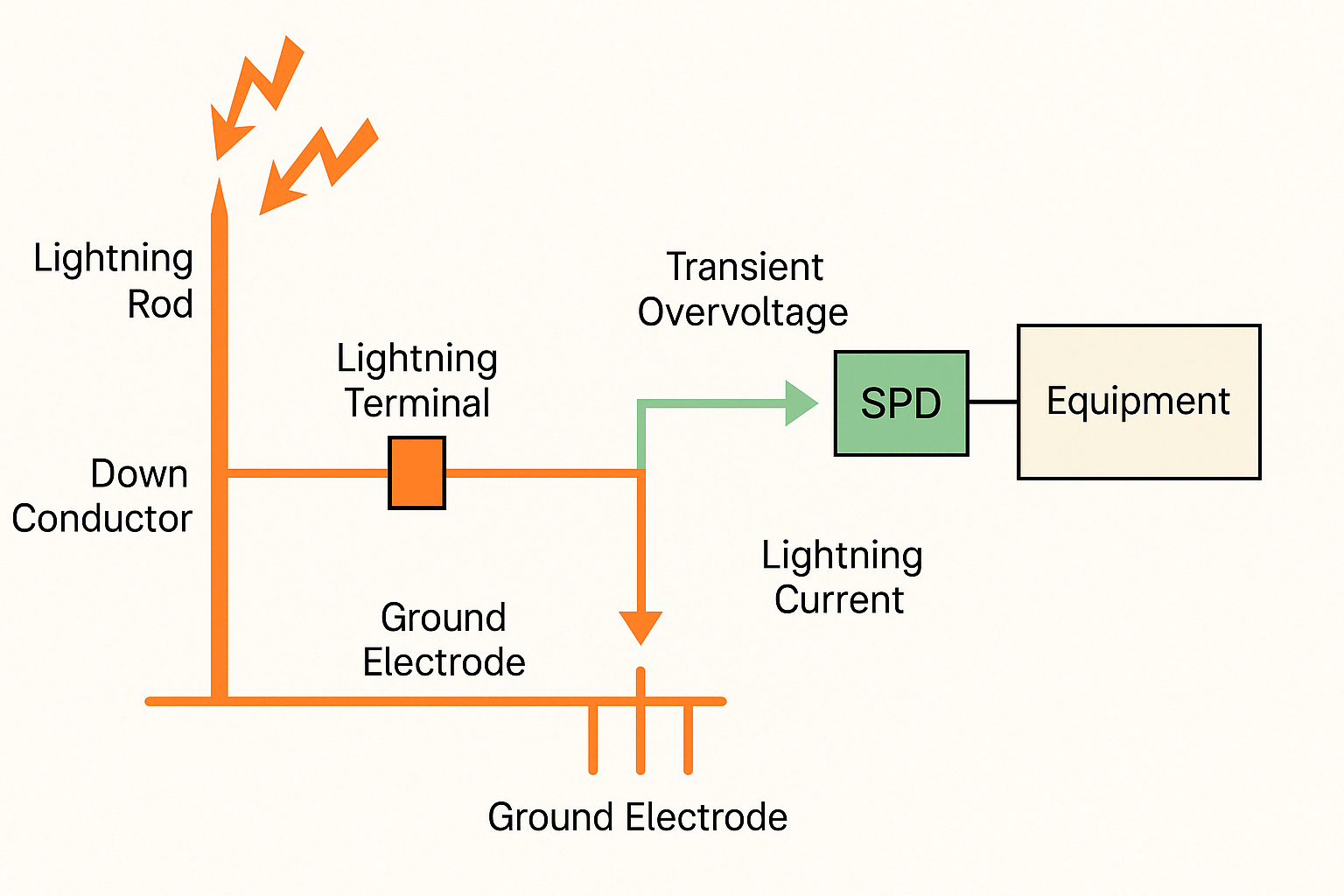
ESD protection leverages the reverse-biased breakdown characteristics of PN junctions, such as diodes, to divert high-voltage transients away from sensitive circuits. The protection circuit remains open during normal operation but conducts during an ESD event via avalanche or Zener breakdown, which is reversible if thermal breakdown is avoided. A series resistor often limits current to prevent thermal damage.
Protection circuits are typically placed near input pads to discharge ESD immediately, minimizing delay. Silicide formation is avoided in ESD regions to maintain higher resistance, enhancing protection without compromising device integrity.
ESD Testing Standards
ESD testing evaluates a device¡¯s robustness using standardized models, primarily:
Human Body Model (HBM)
Simulates charge transfer from a human touching a chip, with a 100pF capacitor and 1.5k¦¸ resistor (MIL-STD-883C Method 3015.7). Classifications include:
- Class 1: <2kV
- Class 2: 2¨C4kV
- Class 3: 4¨C16kV
Machine Model (MM)
Represents discharge from metallic equipment (EIA/JESD22-A115-A), using a 100pF capacitor and zero resistance. Due to low resistance, MM discharges are faster (ms or ¦Ìs) and more damaging, with 200V MM equivalent to 2kV HBM due to higher current.
Testing Methodology
ESD testing mimics gate oxide integrity (GOI) tests, applying incremental voltages (e.g., 3 zaps, starting at 70% of expected threshold, with 50¨C500V steps) and checking for electrical failure. Test configurations include:
- I/O Pins: Test input and output pins separately with positive/negative charges, floating other pins.
- Pin-to-Pin: Apply ESD to one I/O pin, grounding all others while floating inputs/outputs.
- Vdd-Vss: Discharge between power and ground, floating I/O pins.
- Analog Pins: Test differential pairs or op-amp inputs, floating other pins.
ESD Protection in Process and Design
As device scaling reduces junction depths and oxide thicknesses, ESD susceptibility increases. Silicide processes further exacerbate breakdown risks. Protection can be implemented at the fabrication (process) or layout (design) level.
Process-Level ESD Protection
- Source/Drain ESD Implant: Deep N+ implants replace shallow LDD junctions to round sharp corners, reducing electric field concentration and boosting ESD tolerance from <1kV to >4kV. Requires a longer gate to prevent punchthrough and a dedicated SPICE model.
- Contact ESD Implant: A P+ implant beneath the N+ drain lowers breakdown voltage (e.g., 8V to 6V), diverting ESD current before LDD damage, without altering device structure or requiring new SPICE models. Limited to non-silicide processes.
- Salicide Block (SAB): Prevents silicide formation at output MOSFETs, increasing resistance to protect against ESD-induced breakdown (1kV to 4kV), at the cost of an additional photo layer.
- Series Resistor: Adds resistance (e.g., Rs_NW or high-resistance layers) to limit ESD current, a cost-effective alternative to SAB.
Design-Level ESD Protection
Design-level solutions include:
- Gate-Grounded NMOS (GGNMOS): Shorts gate, source, and bulk, allowing the drain-bulk PN junction to avalanche during ESD, triggering the parasitic NPN transistor¡¯s snap-back mode to divert current. PMOS (GDPMOS) operates similarly.
- Multi-Finger Structures: Use parallel fingers to increase current-handling capacity, but non-uniform triggering reduces effectiveness. Solutions include:
- SAB to increase drain resistance for uniform current distribution.
- P+ ESD implant beneath the drain to lower breakdown voltage, enhancing snap-back.
- Gate-Coupled NMOS (GCNMOS): Applies gate voltage to initiate substrate current, enabling uniform finger triggering. However, it risks gate oxide breakdown in smaller devices and is less effective in larger ones.
- Silicon Controlled Rectifier (SCR): Uses a PNPN structure to trigger snap-back and latch-up for protection. Suitable for layout-level design but risks latch-up failure in process-level implementation.
Snap-Back Design Considerations
- NMOS vs. PMOS: NMOS exhibits better snap-back due to higher electron mobility, while PMOS is more ESD-tolerant but less prone to snap-back.
- Trigger and Hold Voltages: Trigger voltage (Vt1) initiates snap-back, between BVCEO and BVCBO. Hold voltage sustains snap-back without entering latch-up, which risks thermal breakdown. Limit current by adjusting W/L ratios or increasing drain/SAB spacing.
Conclusion
ESD protection is critical for IC reliability, using diodes, MOSFETs, parasitic BJTs, and SCRs to divert transients. Process-level solutions like ESD implants and salicide blocks enhance robustness, while design-level techniques like GGNMOS and multi-finger structures optimize protection. Careful management of trigger and hold voltages ensures effective, reusable ESD protection, safeguarding modern electronics from high-voltage transients.
 ALLPCB


