Are you looking to understand the PCB lamination process and how it affects manufacturing time? In short, PCB lamination is a critical step in creating multilayer printed circuit boards, where layers of conductive copper and insulating materials are bonded under heat and pressure. This process can significantly impact production timelines due to factors like material selection, temperature settings, and the number of layers. In this detailed guide, we’ll break down the PCB lamination process steps, explore key variables like materials and temperature, and explain their direct effects on manufacturing time for multilayer boards.
What Is PCB Lamination and Why Does It Matter?
PCB lamination is the process of bonding multiple layers of a printed circuit board (PCB) together to form a single, unified structure. This step is essential for multilayer PCBs, which are widely used in complex electronics like smartphones, medical devices, and industrial equipment. The lamination process ensures electrical connectivity between layers while providing mechanical strength and protection against environmental factors.
The time taken for lamination directly influences the overall manufacturing schedule. A well-optimized lamination process can save hours or even days in production, while issues like improper material choice or temperature control can lead to delays, defects, or rework. Understanding the intricacies of PCB multilayer lamination helps manufacturers and designers plan better and meet tight deadlines.
PCB Lamination Process Steps Explained
The PCB lamination process involves several precise steps to ensure the layers bond correctly without defects. Below, we outline the key stages of PCB multilayer lamination, focusing on how each step contributes to the overall manufacturing time.
1. Preparation of Inner Layers
Before lamination begins, the inner layers of the PCB are prepared. This includes etching the copper foil to create the desired circuit patterns and treating the surface with a chemical process like brown or black oxide. This treatment roughens the copper surface to improve adhesion during lamination. Preparation can take anywhere from 2 to 4 hours per batch, depending on the complexity of the design and the number of layers (typically 4 to 16 for most multilayer boards).
2. Layer Stacking and Alignment
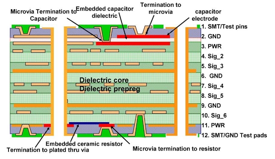
Once the inner layers are ready, they are stacked with insulating materials called prepreg (pre-impregnated resin sheets) placed between them. Prepreg acts as the glue that bonds the layers together. Precision alignment is critical to ensure that vias and traces match across layers. Misalignment can cause electrical failures, requiring rework that adds 12-24 hours to the timeline. This step usually takes 1-2 hours with automated alignment tools.
3. Lamination Under Heat and Pressure
The stacked layers are placed in a lamination press, where they are subjected to high temperature (typically 170-200°C) and pressure (around 200-400 psi). This process cures the resin in the prepreg, bonding the layers into a solid board. The lamination cycle can last 1.5 to 3 hours, depending on the PCB lamination temperature, material thickness, and number of layers. For instance, an 8-layer board might require a longer cycle than a 4-layer board due to increased thermal mass.
4. Cooling and Inspection
After lamination, the board is slowly cooled to prevent warping or internal stress, which can take an additional 1-2 hours. Once cooled, the board undergoes visual and X-ray inspections to check for delamination, voids, or misalignment. If defects are found, the board may need to be scrapped or reworked, adding significant delays (up to 48 hours) to the manufacturing process.
Key Factors Affecting PCB Lamination Manufacturing Time
Several variables influence the duration of the PCB lamination process. By optimizing these factors, manufacturers can reduce production time while maintaining quality. Let’s explore how PCB lamination material, temperature, and other elements impact manufacturing timelines.
1. PCB Lamination Material Selection
The choice of materials plays a huge role in lamination time. Prepreg and core materials come in various resin types, such as epoxy, polyimide, or high-frequency laminates, each with different curing times and thermal properties. For example:
- Standard FR-4 epoxy: Cures in about 1.5-2 hours at 180°C, making it a common choice for cost-effective, quick production.
- High-Tg materials: Require longer curing times (2.5-3 hours) and higher temperatures (up to 200°C) for applications needing better heat resistance.
- Specialty laminates: Used in high-frequency or RF applications, these can extend lamination cycles by 30-50% due to stricter processing requirements.
Choosing the right PCB lamination material based on project needs can save hours in the lamination stage. However, using advanced materials for high-performance boards often means accepting longer manufacturing times.
2. PCB Lamination Temperature Control
Temperature settings during lamination are critical for proper bonding and curing. If the PCB lamination temperature is too low, the resin may not cure fully, leading to weak bonds or delamination. If too high, it can cause resin flow issues or damage to the board, requiring rework. Most presses operate between 170-200°C, with a typical heating rate of 2-5°C per minute to avoid thermal shock. Achieving and maintaining the target temperature can add 30-60 minutes to the process, especially for thicker boards (e.g., 2.0 mm or more) that need uniform heat distribution.
Advanced lamination presses with precise temperature controls can reduce this time by ensuring consistent heating, cutting down potential delays from defective boards.
3. Number of Layers in Multilayer PCBs
The complexity of multilayer PCBs directly affects lamination time. A 4-layer board might complete lamination in under 2 hours, while a 12-layer or 16-layer board could take 3-4 hours due to the increased number of prepreg sheets and copper layers. Each additional layer adds roughly 10-15 minutes to the lamination cycle because of the extra thermal mass and pressure needed for uniform bonding.
For high-layer-count boards, manufacturers often split the lamination into multiple cycles (sequential lamination), which can double or triple the total time. This method, while time-consuming, ensures better quality for complex designs.
How PCB Lamination Impacts Overall Manufacturing Time
Lamination is just one part of the PCB manufacturing process, but its duration and quality affect downstream steps like drilling, plating, and testing. Here’s how delays or optimizations in lamination ripple through the production timeline:
- Defects and Rework: Issues like delamination or voids discovered after lamination can halt production for 1-2 days while the board is repaired or remade. For urgent projects, this can be a costly setback.
- Sequential Processes: Post-lamination steps, such as drilling microvias or applying solder mask, cannot begin until lamination is complete. A 3-hour lamination delay pushes the entire schedule back by at least that much.
- Batch Processing: Manufacturers often laminate multiple boards in a single press cycle to save time. If a batch includes boards with different material or layer requirements, the longest cycle time dictates the pace, slowing down simpler boards.
On the positive side, optimizing lamination—through better material selection, precise temperature control, and automated alignment—can shave off hours per batch. For high-volume orders, this translates to days saved over the entire production run.
Tips for Reducing PCB Lamination Manufacturing Time
For engineers and manufacturers aiming to speed up production without sacrificing quality, consider these practical strategies:
- Choose Compatible Materials: Select PCB lamination materials with similar curing profiles to avoid extended cycles or multiple lamination runs. For standard applications, stick to widely used materials like FR-4 to benefit from faster processing.
- Optimize Design for Fewer Layers: If possible, simplify the PCB design to reduce the number of layers. Fewer layers mean shorter lamination times and lower risks of defects.
- Work with Experienced Partners: Collaborate with a manufacturer that uses modern lamination presses with precise temperature and pressure controls. This minimizes errors and reduces cycle times.
- Plan for Sequential Lamination: For complex boards requiring multiple lamination cycles, account for the added time in your project schedule to avoid unexpected delays.
- Perform Pre-Lamination Checks: Ensure inner layers are clean and properly aligned before lamination to prevent rework. A small investment of 30 minutes in quality checks can save hours later.
Common Challenges in PCB Multilayer Lamination
Even with careful planning, challenges can arise during lamination that extend manufacturing time. Being aware of these issues helps in mitigating their impact:
- Delamination: Poor bonding between layers, often due to incorrect temperature or pressure, can lead to separation. Fixing this requires re-lamination or scrapping the board, adding 1-3 days to the timeline.
- Resin Flow Issues: Excessive or insufficient resin flow during lamination can create voids or uneven thickness, affecting signal integrity (e.g., impedance mismatches of 5-10 ohms). Correcting this may delay production by 24-48 hours.
- Warping: Uneven cooling or improper material selection can cause the board to warp, making it unusable for high-precision applications. Warped boards often need to be remade, costing additional time and resources.
Addressing these challenges requires strict process control and regular equipment maintenance, which, while adding upfront time, prevents larger delays down the line.
Conclusion: Balancing Speed and Quality in PCB Lamination
The PCB lamination process is a cornerstone of multilayer PCB manufacturing, directly influencing both the quality of the final product and the overall production timeline. By understanding the PCB lamination process steps—preparation, stacking, pressing, and cooling—and optimizing factors like PCB lamination material and temperature, manufacturers can significantly reduce PCB lamination manufacturing time. Whether you’re dealing with a simple 4-layer board or a complex 16-layer design, careful planning and attention to detail during lamination ensure faster turnaround without compromising performance.
From selecting the right materials to using advanced equipment for precise control, every decision in the lamination stage has a ripple effect on the manufacturing schedule. By focusing on efficiency and quality, you can streamline production and deliver high-performance PCBs on time for any application.
 ALLPCB


