 ALLPCB


PCB laminate bubbling is a critical issue in printed circuit board manufacturing that can compromise the integrity and performance of electronic devices. This problem often leads to delamination, where layers of the PCB separate, causing failures in functionality. But what causes PCB laminate bubbling, and how can it be prevented? In this comprehensive guide, we'll explore the root causes such as moisture absorption, outgassing, thermal stress, and trapped solvents, while providing actionable solutions to ensure reliable PCB production.
Whether you're an engineer, designer, or manufacturer, understanding these factors is essential for maintaining high-quality circuit boards. Let's dive into the details of PCB laminate issues, when delamination occurs, and how to mitigate risks effectively.
What Is PCB Laminate Bubbling?
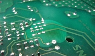
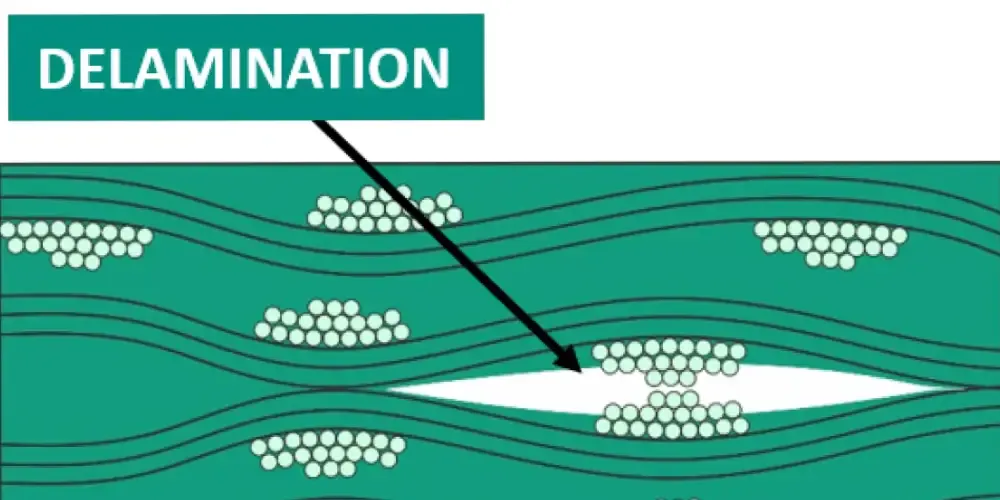
PCB laminate bubbling refers to the formation of air pockets or blisters between the layers of a printed circuit board's laminate material. These bubbles can weaken the bond between layers, leading to delamination—a condition where the layers physically separate. This defect often appears during manufacturing processes like soldering or lamination, or even during the operational life of the board due to environmental factors.
Bubbling is not just a cosmetic issue; it can disrupt electrical connections, reduce mechanical strength, and cause complete board failure. Understanding the causes of delamination in PCB production is the first step to preventing these costly defects.
Common Causes of PCB Laminate Bubbling and Delamination
Several factors contribute to PCB laminate bubbling and the subsequent delamination. Below, we break down the primary causes, including moisture absorption, outgassing, thermal stress, and trapped solvents, to help you identify potential risks in your manufacturing process.
1. Moisture Absorption in PCBs
Moisture absorption is one of the leading causes of laminate bubbling. PCB materials, especially those made from epoxy resins, are prone to absorbing moisture from the environment during storage or processing. When the board is exposed to high temperatures during soldering or reflow processes, the absorbed moisture turns into steam. This steam creates pressure between the layers, forming bubbles and potentially causing delamination.
For instance, if a PCB is stored in a humid environment with relative humidity levels above 60%, it can absorb enough moisture to cause issues during a reflow process at temperatures around 260°C. Studies suggest that even a small moisture content of 0.1-0.2% by weight can lead to significant bubbling under thermal stress.
To mitigate this, proper storage in low-humidity environments (below 30% relative humidity) and pre-baking the boards at 120°C for 2-4 hours before assembly can significantly reduce moisture content.
2. Outgassing During Manufacturing
Outgassing occurs when volatile compounds or gases trapped within the laminate material are released during high-temperature processes. These gases can originate from the resin or prepreg materials used in PCB fabrication. If the gases cannot escape properly, they create bubbles between layers, weakening the bond and leading to delamination.
Outgassing is particularly problematic during the lamination process, where temperatures often exceed 180°C. If the curing process is not optimized, or if low-quality materials with high volatile content are used, the risk of bubbling increases. Manufacturers can address this by selecting materials with low outgassing properties and ensuring proper vacuum lamination to allow gases to escape.
3. Thermal Stress and Temperature Fluctuations
Thermal stress is another major factor in PCB laminate bubbling. During manufacturing and assembly, PCBs are subjected to rapid temperature changes, such as in reflow ovens or wave soldering. These temperature swings cause the materials to expand and contract at different rates due to varying coefficients of thermal expansion (CTE) between the laminate, copper, and other components.
For example, if the CTE mismatch between the laminate (typically 14-17 ppm/°C) and copper (around 17 ppm/°C) is not accounted for in the design, internal stresses build up. This stress can create voids or bubbles, especially if the board undergoes multiple thermal cycles. Delamination often occurs in PCB during these thermal excursions, particularly if the board is not designed with adequate thermal management in mind.
Using materials with compatible CTE values and implementing gradual heating and cooling profiles during assembly can help minimize thermal stress.
4. Trapped Solvents in Laminate Materials
Trapped solvents are a less common but still significant cause of PCB laminate bubbling. During the production of laminate materials, solvents are used to dissolve resins for coating prepreg layers. If these solvents are not fully evaporated during the curing process, they remain trapped within the material. When exposed to high temperatures later, these solvents vaporize, creating bubbles and contributing to delamination.
Manufacturers can prevent this by ensuring thorough curing and drying processes during laminate production. Additionally, quality control checks for residual solvent content can identify potential risks before the material is used in PCB fabrication.
When Does Delamination Occur in PCB?
Delamination in PCB can occur at various stages of the board's lifecycle, from manufacturing to end-use. Understanding these critical points helps in implementing preventive measures. Here are the most common scenarios:
- During Lamination: If the pressure, temperature, or vacuum conditions are not optimized, gases or moisture can get trapped, leading to immediate bubbling or delamination.
- During Soldering or Reflow: High temperatures (often above 250°C) cause moisture or solvents to vaporize, creating internal pressure that separates layers.
- During Operation: Environmental factors like humidity and temperature fluctuations can cause delamination over time, especially in harsh conditions such as automotive or aerospace applications.
- After Storage: Prolonged exposure to humid environments without proper protection can lead to moisture absorption, resulting in delamination during subsequent thermal processes.
By identifying when delamination is most likely to occur, manufacturers can focus on critical control points to reduce risks.
Effects of PCB Laminate Bubbling and Delamination
The consequences of laminate bubbling and delamination go beyond aesthetics. These defects can severely impact the performance and reliability of a PCB. Here are some key effects:
- Electrical Failures: Bubbles and delamination can disrupt traces and vias, leading to open circuits or intermittent connections. This is especially critical in high-frequency applications where signal integrity is paramount.
- Mechanical Weakness: Separated layers reduce the structural integrity of the board, making it prone to cracking or breaking under stress.
- Reduced Lifespan: Delamination accelerates wear and tear, especially in environments with thermal cycling or vibration, shortening the board's operational life.
- Costly Rework or Scrap: Detecting bubbling or delamination often means scrapping entire batches or investing in costly repairs, impacting production budgets.
How to Prevent PCB Laminate Bubbling and Delamination
Preventing PCB laminate bubbling requires a combination of material selection, process control, and environmental management. Below are actionable strategies to minimize the risk of delamination and ensure high-quality boards.
1. Control Moisture Exposure
Store PCB materials and assembled boards in controlled environments with low humidity (below 30%). Use moisture barrier bags with desiccants for long-term storage. Additionally, pre-bake boards at 120°C for 2-4 hours before soldering to remove any absorbed moisture. This step is particularly crucial for boards that have been stored for extended periods.
2. Optimize Lamination and Curing Processes
During lamination, ensure proper vacuum conditions to allow gases to escape. Use controlled temperature and pressure profiles to avoid trapping moisture or solvents. For curing, follow manufacturer guidelines to fully evaporate solvents and cure resins, preventing outgassing issues later.
3. Select High-Quality Materials
Choose laminate materials with low moisture absorption and outgassing properties. Look for materials with compatible CTE values to minimize thermal stress. For high-reliability applications, consider advanced laminates that can withstand multiple thermal cycles without degrading.
4. Manage Thermal Profiles
Design assembly processes with gradual heating and cooling ramps to reduce thermal stress. Avoid exposing boards to unnecessary thermal cycles during testing or rework. For example, limit reflow cycles to the minimum required and ensure peak temperatures do not exceed the material's specifications.
5. Implement Quality Control Checks
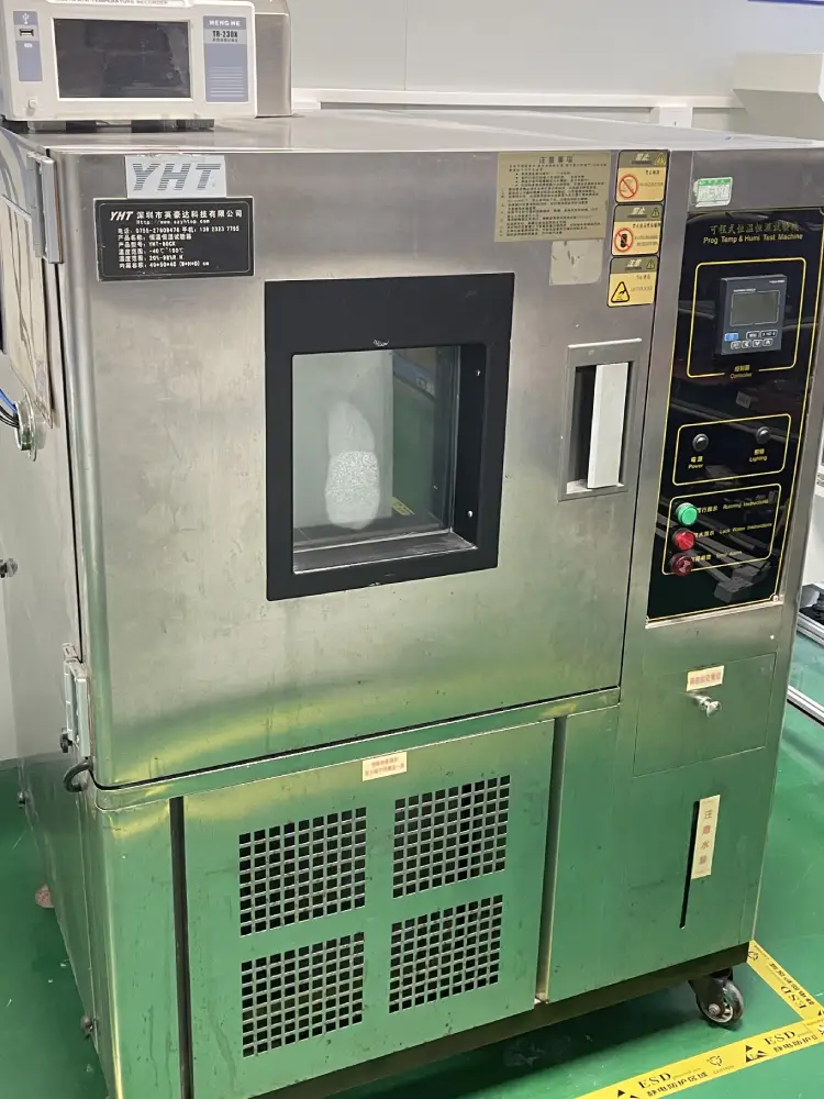
Conduct regular inspections for moisture content, residual solvents, and lamination quality during production. Use techniques like thermal imaging or cross-sectional analysis to detect early signs of bubbling or delamination before they become critical.
Conclusion: Ensuring Reliable PCB Production
PCB laminate bubbling and delamination are preventable issues that require attention to detail in material selection, manufacturing processes, and environmental control. By addressing key causes like moisture absorption, outgassing, thermal stress, and trapped solvents, manufacturers can significantly reduce the risk of defects. Implementing best practices such as pre-baking, optimizing lamination, and using high-quality materials ensures that your PCBs meet the highest standards of reliability and performance.
At ALLPCB, we are committed to supporting engineers and manufacturers with solutions for high-quality circuit board production. By understanding when delamination occurs in PCB and taking proactive steps, you can achieve consistent results and avoid costly failures in your projects. Focus on these strategies to build durable, efficient, and reliable electronic products that stand the test of time.


