 ALLPCB


In the fast-paced world of electronics, maintaining signal integrity in high-speed printed circuit boards (PCBs) is a top priority for designers and engineers. One advanced technique that addresses this challenge is PCB back drilling. But when is back drilling necessary, and how can you ensure it’s done correctly? In this comprehensive guide, we’ll explore the essentials of back drilling, including when to use it, the detailed process, and best practices for via design and signal integrity. Whether you're optimizing a high-speed design or refining PCB design rules, this blog will provide actionable insights to help you achieve top performance.
What is PCB Back Drilling and Why Does it Matter?
PCB back drilling, also known as controlled depth drilling, is a manufacturing technique used to remove unused portions of copper from through-hole vias in a circuit board. These unused portions, often called "via stubs," can cause signal reflections and distortions in high-speed designs. By eliminating these stubs, back drilling enhances signal integrity, reduces noise, and ensures reliable performance in applications where data rates exceed 5 Gbps or even reach up to 25 Gbps in modern systems.
Signal integrity is critical in industries like telecommunications, data centers, and aerospace, where even minor signal distortions can lead to data loss or system failures. Back drilling directly addresses these issues, making it an essential tool for engineers working on cutting-edge technology. In the following sections, we’ll dive into the specifics of when back drilling is necessary and how to implement it effectively.
When to Back Drill: Identifying the Need in Your PCB Design
Back drilling isn’t necessary for every PCB project. It’s a specialized process typically reserved for high-speed designs where signal integrity is paramount. Here are the key scenarios when you should consider back drilling:
- High-Speed Signal Transmission: If your design involves data rates above 5 Gbps, via stubs can create significant signal reflections. For example, a via stub as short as 0.5 mm can introduce impedance mismatches at 10 Gbps, leading to signal degradation. Back drilling removes these stubs to minimize interference.
- Multilayer PCBs with Unused Via Portions: In multilayer boards (often 8 layers or more), through-hole vias may extend beyond the layers they connect, leaving unused copper. This unused section acts as a stub, resonating at certain frequencies and distorting signals. Back drilling is critical in such cases.
- Critical Applications: Designs for servers, networking equipment, or medical devices often require flawless signal performance. Back drilling ensures reliability by reducing electromagnetic interference (EMI) and crosstalk.
- Impedance Control Needs: If your design requires precise impedance matching (e.g., 50 ohms for high-speed differential pairs), via stubs can disrupt this balance. Back drilling helps maintain consistent impedance across signal paths.
However, back drilling isn’t always the answer. For low-speed designs or simpler two-layer boards where vias don’t pose a risk to signal quality, the added cost and complexity of back drilling may not be justified. A good rule of thumb is to simulate your design using signal integrity tools to determine if stubs will impact performance before deciding to back drill.
Understanding PCB Design Rules for Back Drilling
Integrating back drilling into your PCB design requires adherence to specific design rules to ensure manufacturability and performance. These rules help balance the technical needs of signal integrity with the practical constraints of manufacturing. Below are key PCB design rules to follow:
- Define Back Drill Depth Precisely: Specify the exact depth for drilling to avoid damaging active layers. Typically, the back drill should stop 0.2-0.3 mm above the target layer to prevent over-drilling. Use design software to mark these depths clearly in your fabrication files.
- Choose Appropriate Via Sizes: Back drilling requires a slightly larger drill bit than the original via hole to remove the stub. Ensure your via diameter (e.g., 0.3 mm) allows for a back drill bit (e.g., 0.4 mm) without compromising nearby traces or pads.
- Maintain Clearance from Adjacent Features: Keep a minimum clearance of 0.5 mm between back-drilled vias and nearby components or traces to avoid accidental damage during drilling. This clearance also accounts for manufacturing tolerances.
- Document Target Vias: Clearly indicate which vias need back drilling in your design files. Include details like drill depth, diameter, and layer information to prevent errors during production.
- Follow Industry Standards: Adhere to standards like IPC-6012 for PCB fabrication, which provide guidelines on controlled depth drilling and quality control to ensure reliability.
By incorporating these rules into your workflow, you can streamline the back drilling process and avoid costly redesigns or manufacturing defects. Always collaborate closely with your PCB manufacturer to confirm their capabilities and constraints before finalizing your design.
The Back Drilling Process: A Step-by-Step Guide
The back drilling process is a precise manufacturing technique that requires careful planning and execution. Here’s a detailed look at how it’s done, broken down into clear steps:
- Design and Simulation: Begin by simulating your PCB design using signal integrity tools to identify vias with problematic stubs. Focus on high-speed signal paths where data rates exceed 5 Gbps. Mark the vias that require back drilling in your design files.
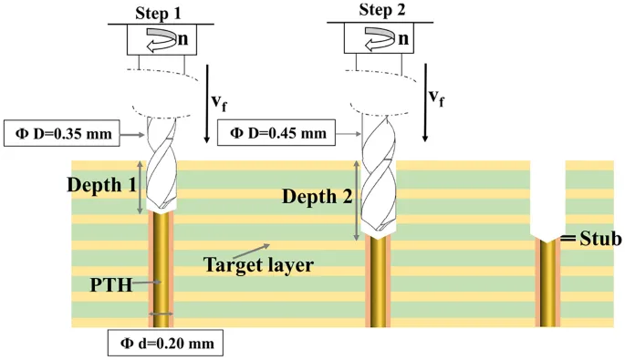
- Fabrication File Preparation: Create detailed documentation specifying the back drill locations, depths, and diameters. For instance, if a via connects layers 1 to 4 in a 12-layer board, specify drilling from layer 12 up to 0.2 mm above layer 4 to remove the stub.
- Initial Via Drilling and Plating: Manufacture the PCB with standard through-hole vias. These vias are drilled and plated with copper to form conductive paths across layers.
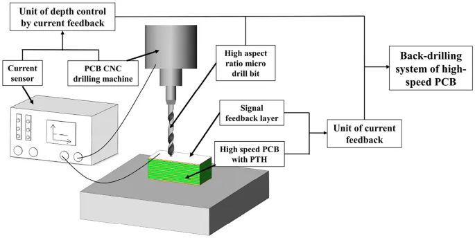
- Controlled Depth Drilling: Use a specialized CNC drilling machine to perform back drilling. A larger drill bit (e.g., 0.1 mm wider than the via) removes the unused copper stub from the opposite side of the board. Depth control is critical—modern machines can achieve tolerances as tight as ±0.05 mm.
- Inspection and Testing: After back drilling, inspect the board using X-ray or automated optical inspection (AOI) to verify that stubs are removed without damaging active layers. Test signal performance on a prototype to confirm improvements in signal integrity.
The precision of back drilling directly impacts its effectiveness. Errors in depth or alignment can compromise via functionality, so strict quality control is essential. Partnering with an experienced manufacturer ensures the process is executed flawlessly.
Signal Integrity Guide: How Back Drilling Improves Performance
Signal integrity is the cornerstone of high-speed PCB design, and back drilling plays a pivotal role in achieving it. Here’s how this technique improves performance, along with practical tips for maximizing results:
- Reduces Signal Reflections: Via stubs act as open-ended transmission lines, reflecting signals back along the path. For a 10 Gbps signal, a stub as short as 0.3 mm can cause a reflection strong enough to corrupt data. Back drilling eliminates this issue by removing the stub.
- Minimizes Crosstalk: Stubs can couple noise between adjacent vias, increasing crosstalk. By removing stubs, back drilling reduces this interference, ensuring cleaner signal transmission.
- Improves Impedance Matching: Stubs introduce impedance discontinuities, disrupting the desired 50-ohm or 100-ohm paths in high-speed designs. Back drilling helps maintain consistent impedance, reducing signal loss.
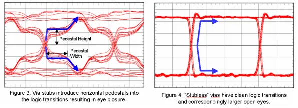
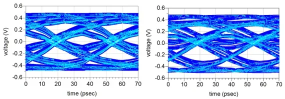
- Enhances Eye Diagram Quality: In high-speed testing, an "eye diagram" visualizes signal quality. Designs with stubs often show a closed or distorted eye due to jitter and noise. Back drilling opens the eye, indicating better performance and reliability.
To maximize signal integrity, combine back drilling with other techniques like proper layer stack-up design, controlled impedance routing, and differential pair matching. Use simulation tools early in the design phase to predict stub effects and prioritize which vias need back drilling.
Via Design Optimization: Best Practices for High-Speed PCBs
Effective via design is critical to complement back drilling and ensure optimal signal integrity. Poorly designed vias can negate the benefits of back drilling, so follow these best practices for via design optimization:
- Minimize Via Stub Length: Even before back drilling, aim to reduce stub length by routing signals to inner layers whenever possible. Shorter stubs mean less material to remove and lower risk of manufacturing errors.
- Use Blind or Buried Vias: In some cases, blind or buried vias (which don’t extend through the entire board) can eliminate stubs entirely, reducing the need for back drilling. However, these options are more expensive, so weigh cost versus benefit.
- Optimize Via Placement: Place high-speed vias away from sensitive components or dense routing areas to simplify back drilling and reduce the risk of damage to nearby features.
- Select Proper Aspect Ratios: Ensure via aspect ratios (depth-to-diameter) are within manufacturing limits, typically below 10:1 for standard processes. This ensures reliable plating and drilling, including back drilling.
- Simulate Via Performance: Use 3D electromagnetic simulation tools to model via behavior at high frequencies. Identify potential resonance issues caused by stubs and address them with back drilling or design adjustments.
Optimized via design, combined with back drilling, creates a robust foundation for high-speed PCBs. Always test prototypes to validate your design choices before moving to full-scale production.
Challenges and Limitations of Back Drilling
While back drilling offers significant benefits, it’s not without challenges. Understanding these limitations helps you make informed decisions and plan accordingly:
- Increased Manufacturing Cost: Back drilling adds an extra step to the production process, increasing costs by 10-20% compared to standard PCB fabrication. Reserve it for designs where signal integrity justifies the expense.
- Precision Requirements: Errors in drill depth or alignment can damage active layers or leave residual stubs, compromising performance. This requires advanced equipment and skilled operators.
- Design Complexity: Incorporating back drilling requires additional planning and documentation, adding time to the design phase. Clear communication with your manufacturer is essential to avoid mistakes.
- Not Suitable for All Boards: Thin boards or those with tight layer spacing may not accommodate back drilling due to the risk of over-drilling. Alternative solutions like blind vias may be needed in such cases.
Despite these challenges, the benefits of back drilling often outweigh the drawbacks for high-speed applications. Careful planning and collaboration with your manufacturing partner can mitigate most issues.
Conclusion: Mastering Back Drilling for Superior PCB Performance
PCB back drilling is a powerful technique for enhancing signal integrity in high-speed designs. By removing via stubs, it minimizes signal reflections, reduces crosstalk, and ensures reliable performance in critical applications. Knowing when to back drill—such as for data rates above 5 Gbps or multilayer boards with unused via portions—is the first step to leveraging this process effectively. Following PCB design rules, understanding the back drilling process, and optimizing via design further ensure success.
For engineers and designers, mastering back drilling means balancing performance needs with manufacturing constraints. Use simulation tools to identify problem areas, adhere to precise design guidelines, and test prototypes to validate results. With these practices, you can achieve superior signal integrity and build PCBs that meet the demands of modern electronics.
By integrating back drilling into your workflow, you’re not just solving a technical challenge—you’re future-proofing your designs for the ever-increasing speeds of tomorrow’s technology. Start applying these insights to your next project and see the difference in performance and reliability.


