ALLPCB


Introduction
Printed circuit board (PCB) X-ray inspection plays a critical role in modern electronics manufacturing by revealing hidden defects that optical methods cannot detect. In high-density assemblies with ball grid arrays (BGAs), chip-scale packages (CSPs), and multi-layer boards, X-ray technology identifies issues like solder voids, bridging, misalignment, and internal cracks without damaging the assembly. However, several X-ray challenges persist, including technical limitations that obscure image clarity and cost concerns that strain production budgets. These hurdles often lead to inconsistent results and increased reliance on skilled personnel for image interpretation. Addressing training requirements and optimizing workflows can unlock the full potential of X-ray inspection in ensuring PCB reliability. This article explores these obstacles and provides factory-driven strategies aligned with industry standards to overcome them.
Understanding PCB X-ray Inspection and Its Importance
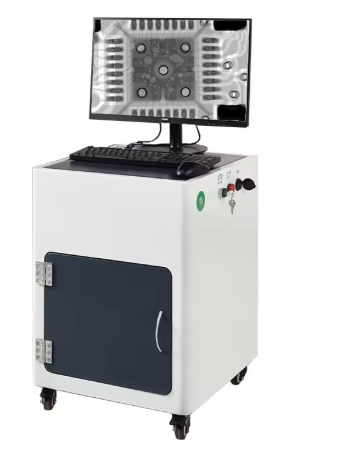
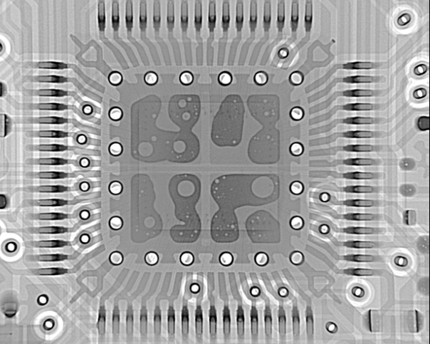
PCB X-ray inspection uses high-energy X-rays passed through the board to create shadow images based on material density and thickness differences. Heavier elements like copper and solder absorb more rays, appearing darker, while lighter materials transmit more, showing lighter shades. Systems range from basic 2D transmission to advanced 3D computed tomography (CT) or laminography, which reconstruct layered views to separate overlapping features. This non-destructive method excels at verifying hidden solder joints, via fills, and barrel cracks in plated-through holes.
In manufacturing, X-ray inspection matters because surface-level checks like automated optical inspection (AOI) miss internal flaws that cause field failures. For class 3 products under IPC-A-610, where high reliability is essential, detecting voids exceeding acceptable limits prevents intermittent connections. Factory teams integrate it post-reflow or after underfill to catch process deviations early, reducing rework costs. Without it, defects escape to functional testing, inflating yield losses in high-volume production.
Key X-ray Challenges in PCB Inspection
Technical Limitations of X-ray Systems
Technical limitations in PCB X-ray inspection often stem from image superposition in 2D systems, where multiple layers blend into a single projection, masking defects like small voids or misaligned vias. High-aspect-ratio boards with dense copper pours create scatter artifacts, reducing contrast and resolution below 5 microns for fine-pitch components. Penetration struggles with thick assemblies or high-atomic-number materials, requiring higher kilovoltage settings that blur finer details. These issues compound in next-generation boards with embedded components, where traditional X-ray fails to resolve sub-micron features reliably. Factories must balance voltage, filtration, and magnification to mitigate these constraints without compromising throughput.
Cost Concerns in Implementing X-ray Inspection
Cost concerns dominate X-ray adoption due to the substantial upfront investment in equipment, often exceeding standard AOI systems by factors of five or more. Maintenance demands specialized service contracts, and operational expenses include radiation shielding and cooling systems to ensure safety compliance. Slower scan times in high-resolution modes create production bottlenecks, necessitating dedicated lines for 100% inspection of critical areas like BGAs. Energy consumption and consumable detectors add recurring costs, particularly in high-volume factories. Smaller operations face amortization challenges over low batch sizes, pushing reliance on outsourced services that introduce lead-time delays.
Training Requirements for X-ray Operators
Training requirements pose a significant barrier, as operators must master system calibration, exposure parameters, and defect recognition across varying board types. Novices struggle with angle adjustments for oblique views, leading to inconsistent image quality and missed defects. Factory programs demand hands-on practice with known good and bad samples to build proficiency in distinguishing process-induced flaws from artifacts. Certification aligned with standards like J-STD-001 ensures repeatability, but high turnover rates necessitate ongoing refreshers. Without robust training, human error amplifies technical limitations, eroding inspection confidence.
Difficulties in Image Interpretation
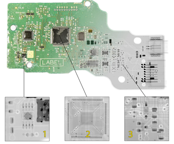
Image interpretation remains one of the most persistent X-ray challenges, especially with noisy images from scatter in leaded components or high-density interconnects (HDI). Operators must differentiate true voids from air gaps, head-in-pillow defects from proper fillet formation, and cracks from edge shadows. Multi-layer overlap confuses via inspection, requiring mental reconstruction that fatigues teams during long shifts. Quantitative analysis, such as void percentage measurement, demands software aids, yet manual verification persists for edge cases. These interpretation hurdles lead to false calls, triggering unnecessary rework and yield impacts.
Practical Solutions and Best Practices for Overcoming X-ray Challenges
Factories overcome technical limitations by transitioning to 3D laminography or CT systems, which slice through layers digitally to eliminate superposition. Adjustable microfocus tubes with 2-10 micron focal spots enhance resolution for fine-pitch BGAs, while automated tilt stages capture multi-angle data for clearer reconstruction. Pre-filtering X-rays reduces scatter, improving signal-to-noise ratios in dense boards. Integrating oblique and transmission modes provides comprehensive views, aligning with IPC-6012 performance specifications for internal integrity.
To address cost concerns, hybrid workflows pair X-ray with AOI: use optical for 90% surface screening, reserving X-ray for high-risk zones like bottom-side BGAs. Statistical sampling based on process capability indices minimizes full-board scans, maintaining throughput above 5 boards per minute. Leasing equipment or cloud-based analysis software lowers capital barriers for mid-volume lines. Preventive maintenance schedules extend tube life, cutting downtime by 30% through vibration monitoring and filament checks.
Robust training programs counter skill gaps with modular curricula covering image interpretation basics to advanced anomaly detection. Simulate factory scenarios using archived datasets, benchmarking against IPC-A-610 criteria for solder joint acceptability. Cross-training with electrical test engineers fosters holistic defect understanding, reducing false positives. Digital twins of inspection setups allow virtual practice, accelerating onboarding from weeks to days.
AI-assisted interpretation tools automate void sizing, crack detection, and alignment checks, alleviating human subjectivity. Machine learning models trained on diverse PCB datasets flag anomalies with 95% accuracy, presenting operators with heatmaps for quick verification. Rule-based software overlays acceptability zones per class levels, streamlining decisions. Factories validate AI outputs against manual audits initially, gradually increasing autonomy to boost efficiency.
Process optimization ties solutions together: establish golden sample libraries for baseline comparisons, implement real-time feedback loops to reflow profiles, and track first-pass yields via statistical process control. Radiation safety protocols, including dosimeters and interlocks, ensure IEC compliance without halting lines. These practices transform X-ray from a bottleneck to a value-adding step in quality control.
Troubleshooting Common Issues in Factory Settings
In production, blurry images often trace to suboptimal kV settings; incrementally test from 60-130 kV based on board thickness to optimize penetration. Persistent scatter in leaded parts responds to copper filters, enhancing contrast without dose hikes. For interpretation disputes, standardize reporting templates with grayscale calibration and magnification rulers. When throughput lags, prioritize programmable recipes for repeat jobs, automating tilt sequences. Cross-reference X-ray findings with cross-sections on outliers to build process correlations, refining thresholds over time.
Conclusion
Overcoming X-ray challenges requires a multifaceted approach blending advanced hardware, rigorous training, and smart workflows tailored to factory realities. Technical limitations yield to 3D imaging, cost concerns ease through hybrids and sampling, while training and AI tackle interpretation hurdles. Standards like IPC-A-610 guide consistent application, ensuring defect detection aligns with reliability goals. Implementing these strategies elevates PCB quality control, minimizing escapes and boosting yields. Electric engineers benefit from proactive integration, turning inspection into a competitive edge in demanding markets.
FAQs
Q1: What are the main technical limitations in PCB X-ray inspection?
A1: Technical limitations include 2D image superposition that obscures multi-layer details, limited resolution for sub-micron features, and scatter artifacts in dense materials. Factories mitigate these with 3D CT or laminography for layer separation and microfocus tubes for sharper contrast. Balancing voltage and filtration prevents penetration issues without blurring. This ensures reliable detection of voids and cracks per industry norms.
Q2: How can factories address cost concerns with X-ray inspection?
A2: Cost concerns arise from high equipment prices and slow throughput, but hybrid AOI-X-ray setups screen surfaces first, reserving X-ray for critical joints. Sampling strategies based on defect rates maintain line speed, while software automation cuts operator needs. Leasing options and maintenance optimization further reduce total ownership costs, making it viable for varied production scales.
Q3: Why are training requirements essential for image interpretation in X-ray challenges?
A3: Training requirements focus on recognizing solder defects like voids versus artifacts, requiring practice with standards-aligned samples. Skilled operators adjust views for optimal clarity and quantify anomalies accurately. Programs reduce variability, preventing false calls that inflate rework. Ongoing certification keeps teams sharp amid evolving board complexities.
Q4: What best practices improve image interpretation during PCB X-ray inspection?
A4: Best practices include AI overlays for void mapping, golden board references, and multi-angle captures to resolve overlaps. Calibrate systems daily for consistent grayscale, and use rule-based software tied to acceptability criteria. Operator checklists standardize reporting, minimizing fatigue errors. These steps enhance accuracy in high-density assemblies.
References
IPC-A-610H — Acceptability of Electronic Assemblies. IPC, 2019
IPC-6012E — Qualification and Performance Specification for Rigid Printed Boards. IPC, 2017
J-STD-001H — Requirements for Soldered Electrical and Electronic Assemblies. IPC, 2020