 ALLPCB


Designing a printed circuit board (PCB) involves many critical decisions, and one of the most important is determining the right trace width. Whether you're working on power traces, high-speed signals, or standard circuits, optimizing PCB trace width is essential for ensuring current capacity, managing trace impedance, and maintaining overall performance in PCB design. In this comprehensive guide, we’ll break down the calculations, standards, and best practices to help you achieve reliable and efficient designs. Let’s dive into the details of PCB trace width and how to make informed choices for your next project.
Why PCB Trace Width Matters in Design
PCB trace width directly impacts how much current a trace can carry, how much heat it generates, and how it affects signal integrity. A trace that’s too narrow for the current can overheat, leading to potential failure or damage. On the other hand, a trace that’s too wide might waste valuable board space or interfere with impedance requirements for high-speed signals. Balancing these factors is key to creating a functional and reliable PCB.
In this blog, we’ll cover the fundamentals of trace width, including how to calculate it based on current capacity and impedance needs, as well as best practices for different applications like power traces and high-speed designs. By the end, you’ll have a clear understanding of how to optimize trace width for your specific requirements.

Understanding PCB Trace Width and Current Capacity
Trace width refers to the physical width of the copper path on a PCB that carries electrical signals or power. The width of a trace determines how much current it can handle without overheating. If a trace is too narrow for the current passing through it, the temperature rises, which can degrade the board material or even cause the trace to burn out.
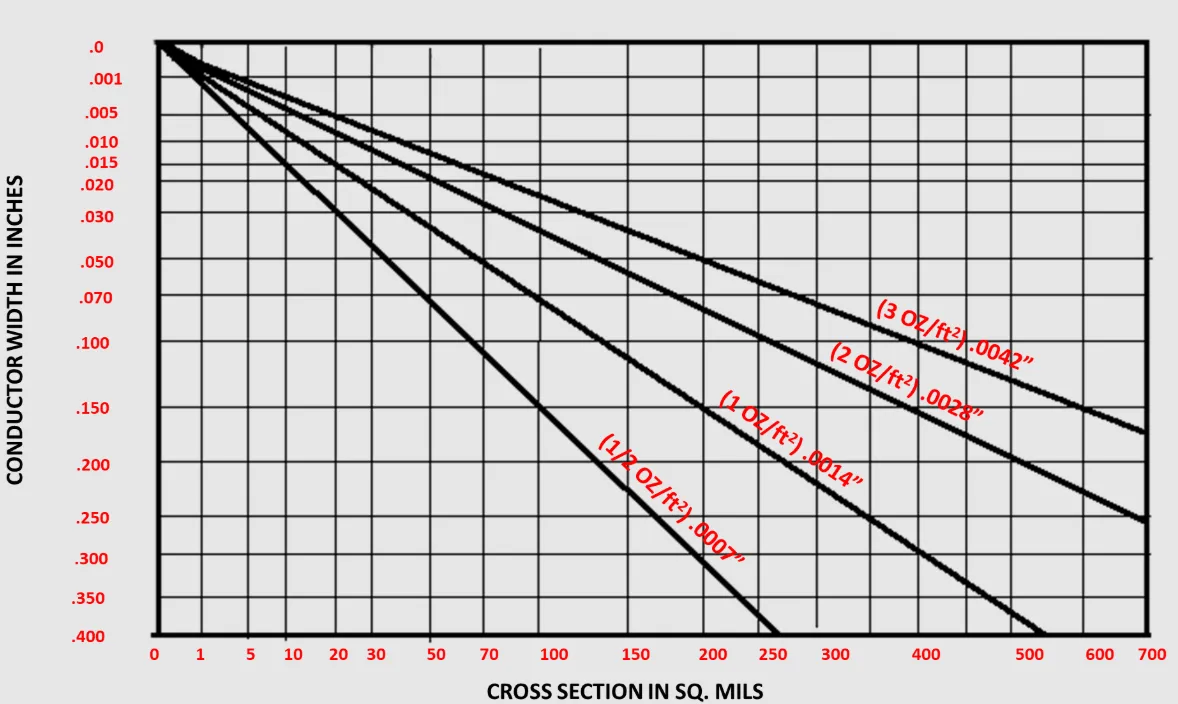
The relationship between trace width and current capacity is influenced by several factors, including the thickness of the copper layer (measured in ounces per square foot), the allowable temperature rise, and the ambient temperature. A common standard for determining trace width based on current is the IPC-2152 guideline, which provides detailed charts and formulas for safe current-carrying capacity.
For example, a 1 oz copper trace (which is about 35 micrometers thick) with a width of 10 mils (0.254 mm) can typically carry around 0.5 amps with a 10°C temperature rise in an internal layer. For higher currents, such as 3 amps, you might need a width closer to 50 mils (1.27 mm) under similar conditions. These values can vary depending on whether the trace is on an external or internal layer, as external traces dissipate heat more effectively.
Calculating PCB Trace Width for Current Capacity
To calculate the appropriate trace width for a given current, you can use formulas derived from industry standards like IPC-2152. However, many designers rely on online calculators for quick and accurate results. Here’s a simplified approach to understanding the process:
- Determine the Current: Identify the maximum current the trace will carry. For power traces, this might be several amps, while signal traces often carry much less.
- Choose Copper Thickness: Standard copper weights are 1 oz, 2 oz, or higher. Thicker copper can handle more current for the same trace width.
- Set Temperature Rise: Decide on an acceptable temperature increase (e.g., 10°C or 20°C). Lower temperature rises require wider traces but keep the board cooler.
- Account for Layer Location: External traces can carry more current than internal ones due to better heat dissipation.
A basic formula for trace width, based on older IPC standards, is:
Width (mils) = (Current (amps) / (k * (Temperature Rise (°C))^b))^ (1/c)
Where k, b, and c are constants depending on the copper weight and layer location. For precise calculations, using a dedicated trace width calculator aligned with IPC-2152 is recommended, as it accounts for more variables and provides updated data.
For instance, if you’re designing a power trace to carry 5 amps with 1 oz copper and a 20°C temperature rise on an external layer, a calculator might suggest a trace width of approximately 100 mils (2.54 mm). Always double-check these values against your specific design constraints and manufacturing capabilities.
Trace Impedance in PCB Design: Why It Matters
Beyond current capacity, trace width also plays a crucial role in controlling impedance, especially for high-speed signals. Impedance is the measure of opposition to the flow of alternating current in a circuit, and it’s critical for maintaining signal integrity in applications like USB, HDMI, or RF designs.
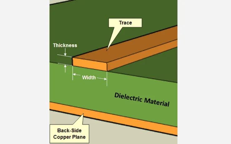
In high-speed PCB design, traces act as transmission lines, and their impedance must match the source and load to prevent signal reflections, which can cause data errors. The characteristic impedance of a trace depends on its width, the thickness of the dielectric material (the PCB substrate), and the distance to the reference plane (usually a ground layer).
For a microstrip trace (a trace on the outer layer with a ground plane beneath), the impedance can be approximated using formulas or calculators. A common target impedance for many high-speed signals is 50 ohms. For a typical FR-4 substrate with a dielectric constant of 4.2 and a height of 0.2 mm to the ground plane, a trace width of about 0.3 mm might achieve 50 ohms. Adjusting the width or dielectric height can fine-tune the impedance.
Best Practices for Optimizing PCB Trace Width
Now that we’ve covered the basics of calculations for current capacity and impedance, let’s explore some practical tips and best practices for optimizing trace width in your PCB designs. These guidelines will help ensure reliability and performance across various applications.
1. Prioritize Power Traces for High Current
Power traces often carry the highest currents on a PCB, so they require wider widths to handle the load without excessive heat buildup. When routing power traces, use the widest possible width within your design constraints. If space is limited, consider using thicker copper (e.g., 2 oz or more) to reduce the required width. Additionally, keep power traces short and direct to minimize voltage drops and heat generation.
2. Use Calculators and Standards for Accuracy
Manually calculating trace width can be error-prone, especially when factoring in variables like temperature rise or impedance. Leverage online tools or software with built-in calculators based on industry standards like IPC-2152. These tools often allow you to input specific parameters and get precise recommendations for your design.
3. Balance Trace Width with Board Space
While wider traces are safer for high currents, they take up more space on the board. In dense designs, this can be a challenge. Optimize your layout by placing high-current traces on outer layers for better heat dissipation, and use vias or multiple layers to distribute current if needed. For signal traces, keep widths as narrow as possible while meeting impedance requirements to save space.
4. Consider Thermal Management
Heat dissipation is a critical factor in trace width design. Wider traces and thicker copper help reduce temperature rise, but you can also improve thermal performance by adding thermal vias, heat sinks, or copper pours near high-current areas. Monitor the expected temperature rise in your calculations to ensure it stays within safe limits for your board material (typically below 20-30°C for most applications).
5. Follow Impedance Guidelines for High-Speed Designs
For high-speed signals, maintaining consistent impedance is more important than maximizing current capacity. Use controlled impedance routing by setting specific trace widths and spacing based on your stack-up. Work closely with your PCB manufacturer to confirm dielectric constants and layer thicknesses, as small variations can affect impedance. Simulation tools can also help predict and adjust for impedance mismatches before fabrication.
6. Account for Manufacturing Tolerances
Trace width can vary slightly during manufacturing due to etching processes. Most manufacturers can achieve tolerances of ±10% or better, but it’s wise to design with some margin. For critical traces, such as those in high-speed or high-current applications, consult with your fabrication partner to understand their capabilities and adjust your design accordingly.
Common Mistakes to Avoid in Trace Width Design
Even experienced designers can make errors when optimizing trace width. Here are some pitfalls to watch out for:
- Underestimating Current Needs: Failing to account for peak currents or transients can lead to undersized traces that overheat. Always design for the worst-case scenario.
- Ignoring Impedance for High-Speed Signals: Using arbitrary trace widths without considering impedance can cause signal reflections and data loss in high-speed circuits.
- Overlooking Heat Dissipation: Placing high-current traces in areas with poor airflow or near heat-sensitive components can cause reliability issues.
- Not Consulting Standards: Relying on outdated rules of thumb instead of current standards like IPC-2152 can result in inaccurate trace sizing.
Tools and Resources for PCB Trace Width Optimization
Fortunately, there are many resources available to simplify trace width calculations and design. Many PCB design software packages include built-in calculators for current capacity and impedance. Additionally, online tools based on industry standards can provide quick estimates for trace width based on your input parameters.
Some popular options include trace width calculators provided by industry organizations or integrated into design platforms. These tools often allow you to specify current, copper weight, temperature rise, and other factors to get accurate recommendations. For impedance control, simulation software can model your PCB stack-up and suggest optimal trace dimensions.
Conclusion: Mastering PCB Trace Width for Better Designs
Optimizing PCB trace width is a fundamental aspect of successful PCB design. By carefully calculating trace width for current capacity and impedance, and following best practices, you can ensure your board performs reliably under all conditions. Whether you’re working on power traces for high-current applications or fine-tuning impedance for high-speed signals, the principles covered in this guide will help you make informed decisions.
Start by using industry standards and calculators to determine the right trace widths for your project. Pay attention to thermal management, board space, and manufacturing tolerances to avoid common pitfalls. With these strategies in mind, you’ll be well-equipped to create efficient and durable PCB designs that meet your performance goals.
Remember, every design is unique, so take the time to analyze your specific requirements and constraints. By prioritizing precision and planning, you can achieve optimal results in your PCB projects.


