When designing a printed circuit board (PCB), one of the most critical decisions you'll face is choosing the right type of via. Vias are essential for creating electrical connections between layers in a multi-layer PCB, but not all vias are created equal. So, what's the difference between microvias and through-hole vias, and which one should you choose for your PCB design? In short, microvias are smaller, ideal for high-density interconnect (HDI) designs, and support compact, modern electronics, while through-hole vias are larger, more robust, and better suited for traditional or high-power applications. This blog will dive deep into a detailed via comparison, exploring the pros, cons, and applications of each type to help you make an informed decision for your next project.
What Are Vias and Why Do They Matter in PCB Design?
Vias are small holes in a PCB that allow electrical signals to pass between different layers of the board. Without vias, multi-layer PCBs would be impossible, as there would be no way to connect traces on different layers. In modern electronics, where space is often limited and performance is critical, choosing the right type of via can impact everything from signal integrity to manufacturing costs.
In this via comparison, we’ll focus on two primary types: microvias and through-hole vias. Each has unique characteristics that make them suitable for different applications, especially when considering high-density interconnect (HDI) technology versus traditional PCB layouts. Understanding their differences will help you optimize your design for performance, cost, and manufacturability.
Understanding Through-Hole Vias: The Traditional Choice
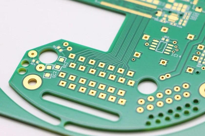
Through-hole vias are the oldest and most traditional type of via used in PCB design. As the name suggests, these vias go straight through the entire thickness of the board, connecting the top layer to the bottom layer and any layers in between. They are typically drilled mechanically using a CNC machine, and their diameter usually ranges from 0.2 mm to 1.0 mm or larger, depending on the design requirements.
Advantages of Through-Hole Vias
- Durability: Through-hole vias are robust and can handle high current loads, making them ideal for power electronics or designs requiring significant thermal dissipation.
- Cost-Effective for Simpler Designs: Since they are easier to manufacture in low-density boards, through-hole vias often have lower production costs for less complex PCBs.
- Wide Compatibility: They work well with through-hole components, which are still used in many industrial and automotive applications due to their reliability under stress.
Disadvantages of Through-Hole Vias
- Larger Size: Their size limits how densely you can pack components on a board, as they take up significant space on all layers, even those not directly connected by the via.
- Signal Integrity Issues: In high-frequency designs, through-hole vias can introduce parasitic capacitance and inductance, leading to signal delays or interference. For instance, a typical through-hole via might add 1-2 pF of capacitance, which can degrade performance at frequencies above 1 GHz.
- Not Ideal for HDI: Due to their size and the need to drill through the entire board, they are less suitable for high-density interconnect designs where space is at a premium.
Applications of Through-Hole Vias
Through-hole vias are commonly used in applications where durability and cost are more important than compactness. Examples include power supply boards, industrial control systems, and older consumer electronics. They are also preferred in prototypes or designs that may require frequent rework, as their larger size makes them easier to inspect and repair.
Exploring Microvias: The Modern Solution for HDI
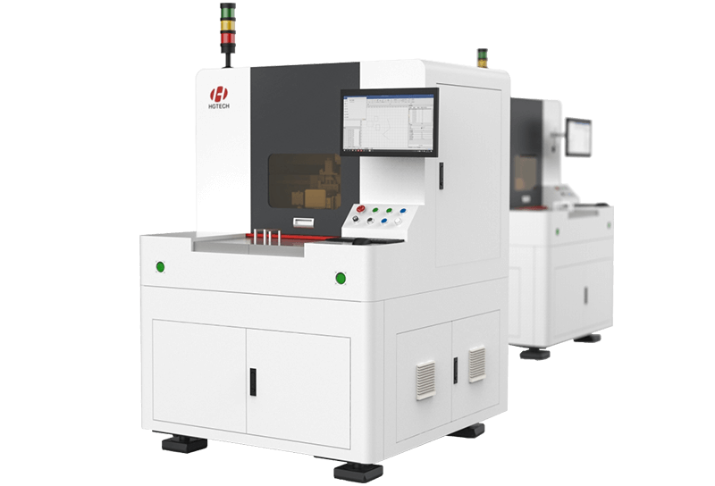
Microvias are a newer innovation in PCB design, specifically developed to meet the demands of high-density interconnect (HDI) technology. Unlike through-hole vias, microvias are much smaller, typically with diameters of 0.1 mm or less, and they are often created using laser drilling rather than mechanical drilling. They usually connect only adjacent layers rather than passing through the entire board.
Advantages of Microvias
- Compact Size: Their small diameter allows for tighter component placement, making them perfect for HDI designs in smartphones, wearables, and other compact devices.
- Improved Signal Integrity: Microvias reduce parasitic effects due to their smaller size, offering better performance in high-speed designs. For example, a microvia might contribute only 0.1-0.3 pF of capacitance, significantly less than a through-hole via, making them suitable for frequencies up to 5 GHz or higher.
- Flexibility in Design: Microvias can be stacked or staggered to create complex layer connections without occupying space on unnecessary layers, optimizing the board layout.
Disadvantages of Microvias
- Higher Manufacturing Cost: The precision required for laser drilling and the complexity of HDI designs often result in higher production costs compared to traditional through-hole vias.
- Lower Current Capacity: Due to their smaller size, microvias are not suitable for high-current applications, as they can overheat or fail under heavy loads.
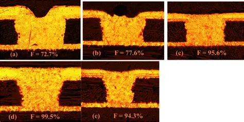
- Reliability Concerns: If not designed or manufactured properly, microvias can be prone to issues like cracking or poor plating, especially in designs with high thermal cycling. Maintaining an aspect ratio (depth-to-diameter) of 0.75:1 or lower is often recommended to ensure reliability.
Applications of Microvias
Microvias shine in applications where space and performance are critical. They are widely used in modern electronics such as smartphones, tablets, medical devices, and IoT products. Their ability to support fine-pitch components like ball grid arrays (BGAs) makes them indispensable in cutting-edge HDI PCB designs.
Via Comparison: Key Differences Between Microvias and Through-Hole Vias
To help you choose the right via for your PCB design, let’s break down the key differences between microvias and through-hole vias across several critical factors:
| Factor | Microvias | Through-Hole Vias |
|---|---|---|
| Size | Small (0.1 mm or less) | Larger (0.2 mm to 1.0 mm or more) |
| Manufacturing Method | Laser drilling | Mechanical drilling |
| Layer Connection | Adjacent layers only (unless stacked) | Through entire board |
| Signal Integrity | Better for high-speed (low capacitance, ~0.1-0.3 pF) | Poorer for high-speed (higher capacitance, ~1-2 pF) |
| Current Capacity | Lower, not ideal for high power | Higher, suitable for power applications |
| Cost | Higher due to precision manufacturing | Lower for simpler designs |
| Best Use Case | HDI designs, compact electronics | Traditional, high-power, or industrial designs |
This via comparison highlights that neither type is inherently "better"—the right choice depends on your specific design needs. If you're working on a compact, high-speed device, microvias are likely the way to go. For a rugged, high-power application, through-hole vias may be more appropriate.
When to Use Microvias in HDI PCB Design
High-density interconnect (HDI) technology is all about packing more functionality into smaller spaces, and microvias are the backbone of this approach. Here are some scenarios where microvias are the clear choice:
- Space Constraints: If your design requires a small form factor, such as in wearable tech or mobile devices, microvias allow for tighter routing and finer pitch components.
- High-Speed Signals: For applications like 5G devices or high-performance computing, microvias minimize signal loss and interference, supporting faster data rates.
- Complex Multi-Layer Designs: Microvias enable connections only where needed, reducing clutter on inner layers and allowing for more efficient use of board space in designs with 8 or more layers.
However, keep in mind the importance of design rules for microvias. Maintaining a low aspect ratio (e.g., 0.75:1) and ensuring sufficient drill-to-copper clearance (typically 7-8 mils) can prevent manufacturing defects and ensure reliability.
When to Opt for Through-Hole Vias in PCB Design
While microvias dominate modern HDI designs, through-hole vias still have their place in many applications. Consider using them in these situations:
- High-Power Applications: If your design involves significant current, such as in power converters or motor control systems, through-hole vias can handle the load without overheating.
- Cost-Sensitive Projects: For simpler, low-density boards where compactness isn’t a concern, through-hole vias are often cheaper to manufacture.
- Harsh Environments: In industrial or automotive applications where the PCB may face vibration, thermal stress, or mechanical shock, the durability of through-hole vias offers an advantage.
Practical Tips for Choosing the Right Via in PCB Design
Selecting between microvias and through-hole vias requires balancing several factors. Here are some actionable tips to guide your decision:
- Analyze Your Design Requirements: Determine the key priorities—space, speed, power, or cost—and choose the via type that aligns with those needs.
- Consider Signal Frequency: For high-frequency designs above 1 GHz, microvias are almost always the better choice due to their lower parasitic effects.
- Evaluate Manufacturing Capabilities: Ensure your PCB manufacturer can handle the precision required for microvias if you opt for HDI technology, as not all facilities are equipped for laser drilling.
- Plan for Thermal Management: If heat dissipation is a concern, through-hole vias or a hybrid approach combining both via types might be necessary.
- Test and Validate: Use simulation tools to model signal integrity and thermal performance with your chosen via type before finalizing the design.
Conclusion: Making the Right Choice for Your PCB Design
Choosing between microvias and through-hole vias is a pivotal decision in PCB design that can affect everything from performance to cost. Microvias are the go-to option for high-density interconnect (HDI) designs, offering compact size and excellent signal integrity for modern, high-speed electronics. On the other hand, through-hole vias remain a reliable choice for traditional, high-power, or cost-sensitive applications where durability is key.
By understanding the strengths and limitations of each via tChoose between microvias and through-hole vias for your PCB design. Learn the pros, cons, and ideal applications of each via type for HDI and traditional boards.ype through this via comparison, you can make an informed decision tailored to your specific project needs. Whether you're designing the next cutting-edge wearable device or a robust industrial system, selecting the right via will ensure your PCB performs optimally while meeting manufacturing and budget constraints.
At ALLPCB, we’re committed to supporting your PCB design journey with high-quality manufacturing solutions for both HDI and traditional designs. Explore our services to bring your innovative ideas to life with precision and reliability.
 ALLPCB


